Module 6
Logical Synthesis
Synthesis Basics - Topics
DC Execution - Topics
Genus Execution - Topics
TOPIC 1: WHAT IS SYNTHESIS (DEEP, FROM ZERO)
1. Why do we need synthesis at all?
A student writes RTL code like this:
always @(posedge clk)
q <= a & b;
Question Can silicon understand this code? Can fabrication people manufacture always @ or & operator?
NO
Silicon understands only:
- Gates (AND, OR, INV)
- Flip-flops
- Wires
So someone must convert RTL into gates. That someone is called SYNTHESIS.
2. SIMPLE & INDUSTRY-CORRECT DEFINITION
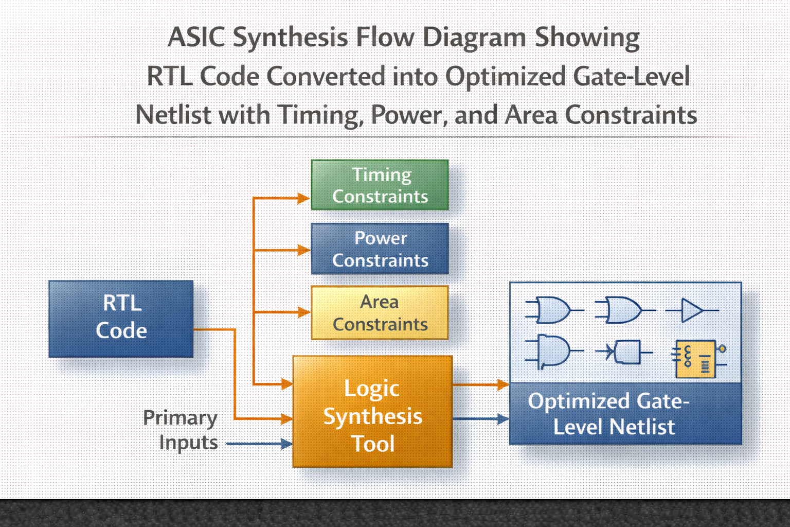
Synthesis is a process of converting RTL code into an optimized gate-level netlist by applying design constraints such as timing, power, and area, so that the design can be physically implemented on silicon.
3. What synthesis is NOT (important clarity)
Synthesis is NOT:
- Simulation
- Verification
- Fabrication
- Physical design
Synthesis does not place gates, does not route wires.
It only decides:
- Which gates?
- How many?
- How fast?
- How optimized?
4. Real-life analogy (VERY IMPORTANT FOR STUDENTS)
RTL = Recipe
Synthesis = Chef
Gates = Ingredients
Example You say:
“Make biryani in 30 minutes with less oil”
Chef decides:
- How much rice?
- How much spice?
- Cooking method?
Similarly:
RTL says:
y = a + b;
Constraints say:
- Finish in 1ns
- Low power
- Small area
Synthesis decides:
- Which adder?
- Ripple adder or CLA?
- High drive or low drive?
5. What exactly goes INTO synthesis?
Synthesis does NOT work blindly.
It needs:
- RTL → What logic to build
- .lib → What gates are available
- .sdc → How fast & how optimized
Without ALL THREE, synthesis cannot work.
6. What exactly comes OUT of synthesis?
After synthesis, you get:
Gate-level netlist
AND2_X1 U1 (.A(a), .B(b), .Y(n1));
DFF_X1 U2 (.D(n1), .CK(clk), .Q(q));
This file can be:
- Placed
- Routed
- Fabricated
RTL cannot.
7. What happens INSIDE synthesis (conceptual, not headlines)
Synthesis internally does three BIG jobs:
1. Understand logic
RTL → Boolean equations
2. Optimize logic
Remove:
- Redundant logic
- Unused logic
- Slow paths
3. Map logic
Boolean logic → Real gates from .lib
This happens automatically, based on constraints.
8. Very small RTL → synthesis example (CLEAR)
RTL:
assign y = a & b;
Library has:
- AND2_X1 (slow, small)
- AND2_X4 (fast, big)
Constraint:
create_clock -period 1
Tool thinks:
“1ns is tight → use AND2_X4”
If clock = 10ns:
“Relaxed → use AND2_X1”
THIS is synthesis intelligence
9. Why synthesis optimization is REQUIRED
If synthesis did not optimize:
- Chip would be too slow
- Too large
- Too hot (power)
Manufacturing cost increases Product fails
So synthesis is mandatory, not optional.
11. Student takeaway (CRITICAL)
After this topic, a student must remember:
RTL is human readable Gates are silicon readable Synthesis is the translator + optimizer + Mapping Constraints control synthesis decisions
If a student understands this → foundation is strong.
TOPIC 2: TYPES OF SYNTHESIS (FROM ZERO, VERY CLEAR)
Before going deep, remember one golden rule:
Synthesis is NOT a single step. It has TYPES depending on HOW MUCH physical information is known.
1. Why do we need “types” of synthesis?
Think like this
When you write RTL, you don’t know:
- Where gates will be placed
- How long wires will be
- How congested the chip will be
So synthesis is done in levels.
Just like:
- School → College → Job
Each level has more real-world constraints.
2. Main Types of Synthesis (Industry View)
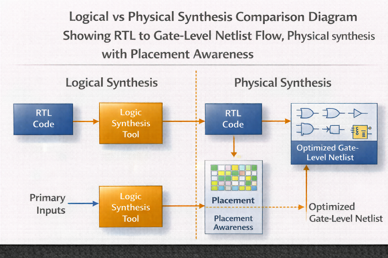
There are TWO MAIN TYPES:
1. Logical Synthesis 2. Physical Synthesis
This is NOT book language — this is industry language
3. Logical Synthesis (MOST IMPORTANT FOR BEGINNERS)
What Logical Synthesis means (CLEAR definition)
Logical synthesis is the process of converting RTL into an optimized gate-level netlist using timing, power, and area constraints, WITHOUT considering actual physical placement and routing.
Key point No placement, no routing, no wire lengths
What logical synthesis KNOWS:
- RTL logic
- Gate delays from .lib
- Clock constraints from .sdc
What logical synthesis DOES NOT know:
Exact wire length Cell placement Congestion
So it assumes ideal conditions.
4. What exactly happens in Logical Synthesis (INSIDE TOOL)
Step by step (student must visualize this):
STEP 1: RTL is read
assign y = (a & b) | c;
STEP 2: Boolean equation is created
y = (a AND b) OR c
STEP 3: Optimization happens
- Can logic be simplified?
- Can gates be shared?
- Can delay be reduced?
STEP 4: Mapping happens
Logic → Standard cells from .lib
5. Example (VERY IMPORTANT)
RTL:
assign y = a & a;
What student wrote:
AND gate
What synthesis does:
y = a
AND gate removed Why? Because a & a = a
This is logical optimization
6. Why Logical Synthesis is REQUIRED
If we skip logical synthesis:
- Design too slow
- Area too big
- Power too high
PNR tools expect: ✔ Clean ✔ Optimized ✔ Gate-level netlist
RTL cannot be given directly to PNR.
7. Advantages of Logical Synthesis
Fast execution Early timing estimation Catches RTL issues early Reduces logic complexity Industry standard first step
8. Disadvantages of Logical Synthesis (VERY IMPORTANT)
No real wire delay Timing may change after placement Congestion not visible Clock skew not accurate
That’s why Physical Synthesis exists.
9. Physical Synthesis (HIGH-LEVEL, not deep yet)
Simple definition:
Physical synthesis is synthesis performed with placement awareness, where gate optimization considers real wire lengths and congestion.
Logical synthesis = assumption Physical synthesis = reality
We will cover this later in detail.
Comparison Table (Student Friendly)
Feature | Logical Synthesis | Physical Synthesis |
Placement aware | No | Yes |
Wire delay | Estimated | Realistic |
Speed | Faster | Slower |
Accuracy | Medium | High |
Used when | Early stage | Later stage |
1.2. Student Conclusion (VERY IMPORTANT)
A student should remember:
✔ Logical synthesis = logic + constraints ✔ Physical synthesis = logic + constraints + placement ✔ Logical synthesis ALWAYS comes first ✔ Physical synthesis refines it
TOPIC 3: TRANSLATION IN LOGICAL SYNTHESIS (FROM ZERO)
This is the first real internal step of logical synthesis. Most students don’t understand it — now you will
1. What is Translation? (Very clear definition)
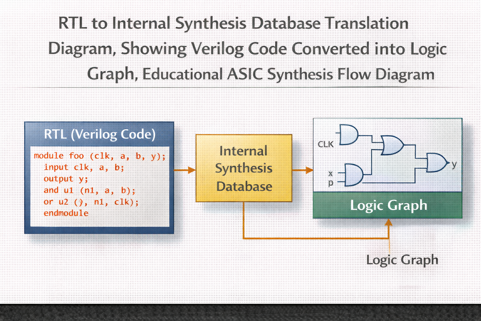
Translation is the process where the synthesis tool converts RTL code (Verilog/VHDL) into an internal Boolean and data-structure representation that the tool can understand and manipulate.
Key idea Tool does NOT work directly on Verilog text It first converts RTL into its own internal model
2. In which stage of synthesis does Translation happen?
Translation happens at the VERY BEGINNING of Logical Synthesis.
Logical Synthesis Flow (high level):
1. Translation 2. Optimization 3. Technology Mapping 4. Netlist Generation
So remember clearly:
Translation = FIRST STEP
3. Why Translation is required?
Humans understand RTL like this:
assign y = (a & b) | c;
But tools understand logic like:
Node1 = AND(a, b)
Node2 = OR(Node1, c)
So translation:
- Removes syntax
- Builds logic graph
- Creates internal data structures
Without translation → No optimization → No mapping → No synthesis
4. What exactly happens during Translation? (Internals)
During translation, the tool:
✔ Parses RTL syntax ✔ Checks syntax errors ✔ Identifies modules, ports, wires, regs ✔ Builds Boolean equations ✔ Creates RTL database / design database
At this stage:
- No optimization
- No gates
- No timing improvement
Only understanding the design
5. Simple Example (VERY IMPORTANT)
RTL Code:
module and_or (
input a, b, c,
output y
);
assign y = (a & b) | c;
endmodule
After Translation (Conceptual):
Design DB:
Inputs: a, b, c
Output: y
Logic:
t1 = a AND b
y = t1 OR c
Still no NAND, NOR, INV Only logic relationships
6. Commands related to Translation (Industry tools)
In Synopsys Design Compiler (example):
analyze -format verilog and_or.v
elaborate and_or
OR (new style):
read_verilog and_or.v
analyze → parses RTL elaborate → builds design hierarchy read_verilog → does both together
(We will explain analyze vs elaborate vs read_verilog later in detail)
7. Errors caught during Translation
This stage catches:
Syntax errors Missing modules Port mismatches Width mismatches Unresolved references (we’ll cover later)
So translation = RTL sanity check
9. Student-Level Summary
A student should remember:
✔ Translation is the first step of logical synthesis ✔ RTL is converted into tool-understandable logic ✔ No optimization happens here ✔ Commands: analyze, elaborate, read_verilog ✔ Errors are caught early
TOPIC 4: OPTIMIZATION IN LOGICAL SYNTHESIS (FROM ZERO)
This is the heart of synthesis. Most beginners think synthesis = conversion. No. Synthesis = OPTIMIZATION
1. What is Optimization? (Clear & Practical Definition)
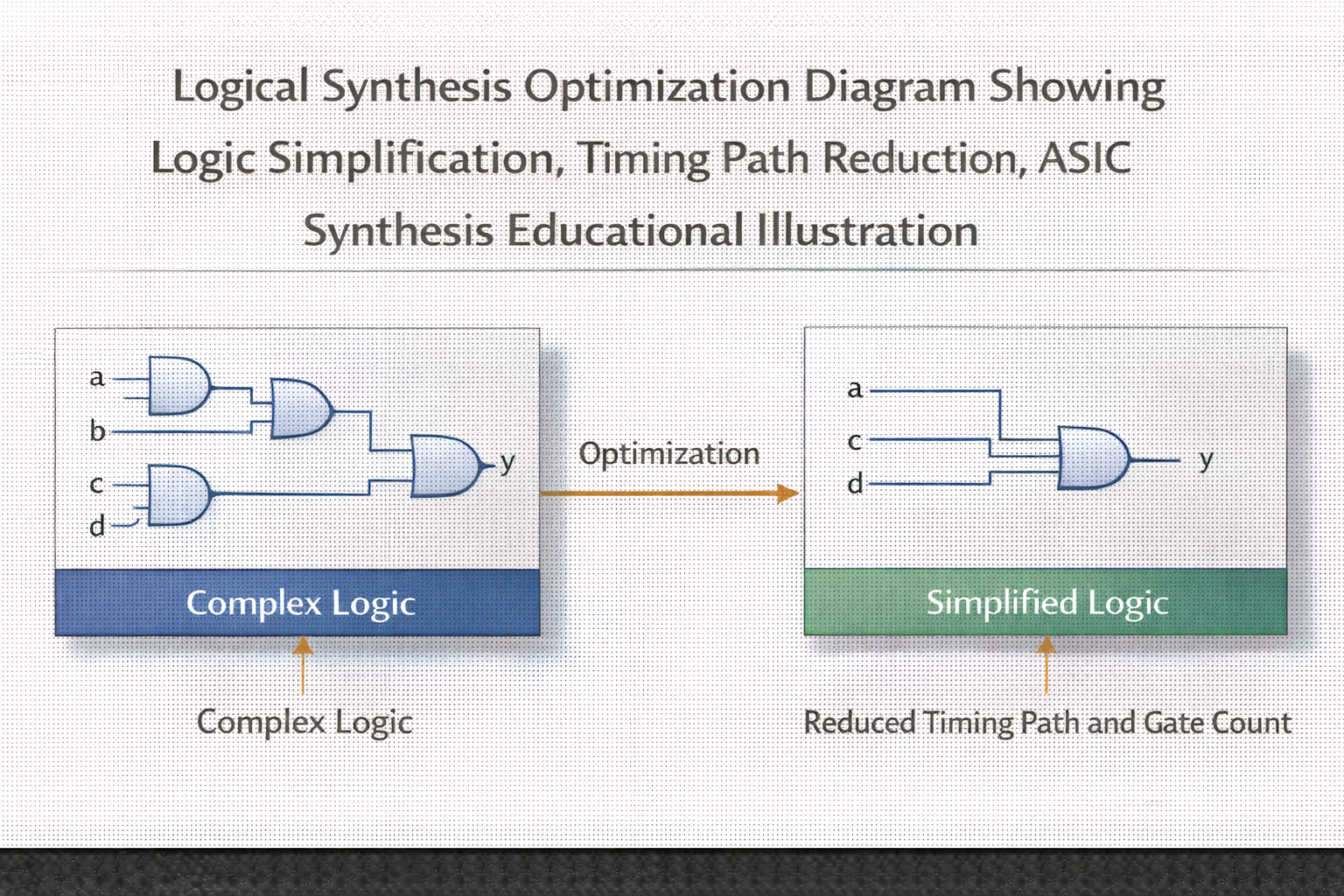
Optimization is the process of modifying the translated RTL logic to achieve the best possible timing, area, and power while still maintaining the same functionality.
Simple words for students Same output Less delay Less gates Less power
2. Why Optimization is Needed? (Real-life example)
Imagine you write RTL like this:
assign y = a & b;
assign z = a & b;
Functionally correct But hardware result :
- Two AND gates
- Same inputs
- Waste of area & power
Optimization will:
wire t = a & b;
assign y = t;
assign z = t;
✔ One AND gate ✔ Less area ✔ Less power
3. When does Optimization happen in synthesis?
Logical Synthesis Flow (updated):
1. Translation 2. Optimization 3. Mapping 4. Netlist generation
So optimization happens AFTER translation and BEFORE mapping.
4. Types of Optimization (VERY IMPORTANT)
Optimization is driven by constraints.
1. Timing Optimization
Goal: Make design faster
Examples:
- Reduce logic depth
- Balance paths
- Restructure logic
2. Area Optimization
Goal: Use fewer gates
Examples:
- Remove duplicate logic
- Share common expressions
3. Power Optimization
Goal: Reduce switching activity
Examples:
- Remove unnecessary toggles
- Clock gating (we’ll cover later)
Tool tries to balance Timing ↔ Area ↔ Power
5. Example: Timing Optimization (Clear)
RTL:
assign y = ((a & b) | (c & d)) & e;
Logic depth = 3 levels
Tool may restructure logic internally to:
- Reduce critical path
- Balance gates
You don’t change RTL Tool changes structure internally
6. Optimization Techniques (What tool actually does)
During optimization, tool performs:
✔ Boolean simplification ✔ Constant propagation ✔ Dead logic removal ✔ Logic sharing ✔ DeMorgan transformations ✔ Path restructuring
Example:
assign y = a & 1'b1;
Optimized to:
assign y = a;
7. Optimization is Constraint Driven (Very Important)
Without constraints:
- Tool does minimum work
- No guarantee of timing
Constraints guide optimization:
- .sdc tells tool what to optimize for
Example:
set_clock_uncertainty 0.2
set_max_delay 5
Tool now knows: “I MUST make design fast”
8. What Optimization is NOT
Not technology mapping Not gate selection Not placement aware
It is still technology-independent logic optimization.
9. Commands Related to Optimization
Optimization happens during:
compile
or advanced:
compile_ultra
You don’t manually say “optimize this AND gate” Tool decides automatically
1.1. Student-Level Summary
✔ Optimization improves timing, area, power ✔ Happens after translation ✔ Same function, better hardware ✔ Driven by constraints ✔ Uses Boolean simplification & restructuring
TOPIC 5: MAPPING (TECHNOLOGY MAPPING)
Till now:
- RTL ✔
- Translation ✔
- Optimization ✔ (technology-independent)
Now comes the MOST CRITICAL STEP in logical synthesis.
1. What is Mapping? (Best Beginner Definition)
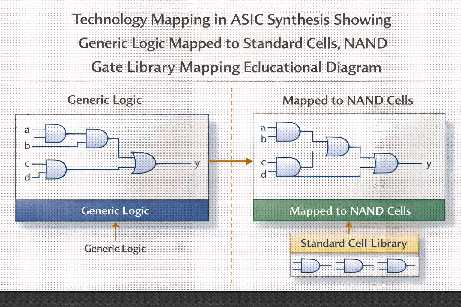
Mapping is the process of converting the optimized generic logic into actual standard cells (gates) available in the target technology library (.lib).
In simple student language Till now, tool knows only AND, OR, NOT (abstract logic) After mapping, tool knows real gates like NAND2_X1, DFF_X2, AOI21_X4
Without mapping → no real hardware
2. Why Mapping is Needed? (Very Important Question)
RTL says:
assign y = a & b;
But fabrication factory does NOT understand:
- &
- |
Factory understands only:
- standard cells from a library
Example:
NAND2_X1
NOR2_X2
INV_X4
DFF_X1
Mapping connects logic → real silicon gates
3. Where Mapping Happens in Synthesis Flow?
Logical Synthesis Flow (updated):
1. RTL 2. Translation 3. Optimization 4. Mapping 5. Gate-level netlist generation
4. What Does Tool Use for Mapping?
Standard Cell Library (.lib)
This file contains:
- Gate functionality
- Delay
- Area
- Power
- Drive strength
Example cells:
NAND2_X1
NAND2_X2
NAND2_X4
Same function, different strength & delay.
5. Simple Mapping Example (Clear)
RTL:
assign y = a & b;
Tool Decision:
AND gate not available But NAND + INV available
Mapped result:
NAND2_X1 → INV_X1
Hardware wise:
y = NOT (a NAND b)
Function same ✔ Uses available cells ✔
6. Mapping is Constraint Driven (Again!)
Mapping depends on:
- Timing constraints
- Area constraints
- Power constraints
Example:
If timing is tight:
NAND2_X4 (faster, bigger)
If area is critical:
NAND2_X1 (slower, smaller)
Tool automatically decides.
7. What Exactly Happens During Mapping?
Tool performs:
✔ Cell selection ✔ Drive strength selection ✔ Gate restructuring ✔ Delay balancing
Example: Instead of one slow gate: Tool may use two faster gates
8. Commands Related to Mapping
Mapping is performed during:
compile
or
compile_ultra
But mapping needs library first:
set target_library "slow.lib"
set link_library "* slow.lib"
Without .lib: Mapping fails No gate-level netlist
9. Gate-Level Netlist After Mapping
Before mapping (generic):
AND
OR
NOT
After mapping:
NAND2_X1
INV_X2
DFF_X1
This is what PNR understands later.
1.1. Student Summary
✔ Mapping converts logic → real gates ✔ Uses .lib file ✔ Happens after optimization ✔ Produces gate-level netlist ✔ Decides speed, area, power
TOPIC 6: RTL vs GATE-LEVEL NETLIST
& Why RTL is NOT Used as PNR Input
This topic is EXTREMELY IMPORTANT for students. Many beginners get confused here.
1. What is RTL? (Quick Recall – in Simple English)
RTL (Register Transfer Level) describes:
- What logic should do
- How data flows between registers
- Written by humans
Example:
always @(posedge clk)
q <= d;
RTL:
- Abstract
- Technology-independent
- No physical meaning
2. What is Gate-Level Netlist?
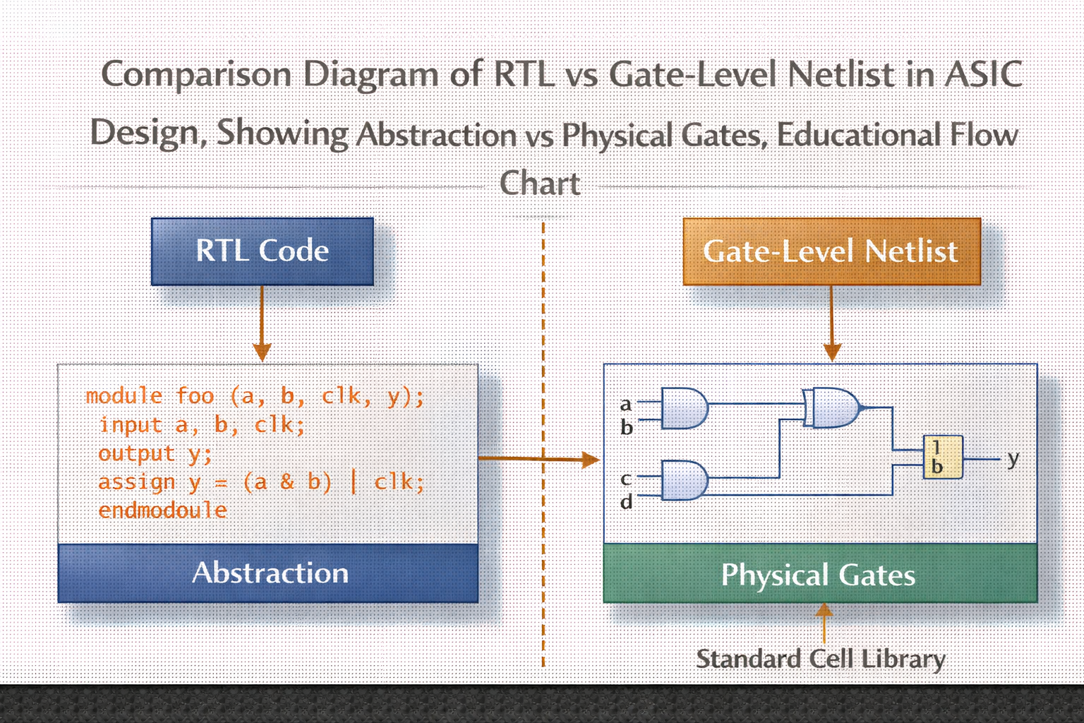
Gate-level netlist is the synthesized output where the design is described using real standard cells from a technology library.
Example:
DFF_X1 U1 ( .D(d), .CLK(clk), .Q(q) );
Gate-level netlist:
- Uses real gates
- Technology-dependent
- Ready for physical design
3. Key Differences (STUDENT MUST MEMORIZE)
Aspect | RTL | Gate-Level Netlist |
Written by | Designer | Synthesis tool |
Abstraction | High | Very low |
Gates | Not shown | Explicit gates |
Technology | Independent | Dependent (.lib) |
Timing info | No | Yes (cell delays) |
Used for PNR? | NO | YES |
4. Why RTL Cannot Be Used for PNR? (Very Important)
PNR needs:
- Exact gate locations
- Exact delays
- Exact connectivity
- Exact cell dimensions
RTL does NOT have:
Cell size Delay Power Drive strength
PNR tools cannot place always blocks or assign statements
5. Real-Life Example (BEST FOR STUDENTS)
Think like this:
RTL = House Blueprint
- “Room here”
- “Door there”
Gate Netlist = Bricks + Cement
- Brick size
- Wall thickness
- Material type
You cannot build a house from only blueprint You need bricks → same as PNR needs gates
6. What Exactly PNR Expects as Input?
PNR expects:
- Gate-level netlist
- Timing constraints (SDC)
- Technology LEF
- Physical libraries
RTL gives NONE of these.
7. Example Comparison (Clear)
RTL:
assign y = a & b;
Gate-level:
NAND2_X1 U1 ( .A(a), .B(b), .Y(n1) );
INV_X1 U2 ( .A(n1), .Y(y) );
PNR understands: ✔ NAND ✔ INV assign
9. Student Conclusion
✔ RTL = functional description ✔ Gate netlist = real hardware ✔ PNR works only on gate-level ✔ Synthesis bridges RTL → gates
TOPIC 7: INPUTS OF LOGICAL SYNTHESIS
(VERY IMPORTANT – Students must clearly understand this)
Logical synthesis cannot start without proper inputs. If any input is wrong or missing → synthesis result will be wrong.
1. What Are the Inputs of Logical Synthesis?
Logical synthesis mainly needs THREE mandatory inputs:
- RTL (Design description)
- Technology Library (.lib)
- Timing Constraints (.sdc)
Optional but commonly used:
- UPF / CPF (for low power)
- Design constraints (.tcl)
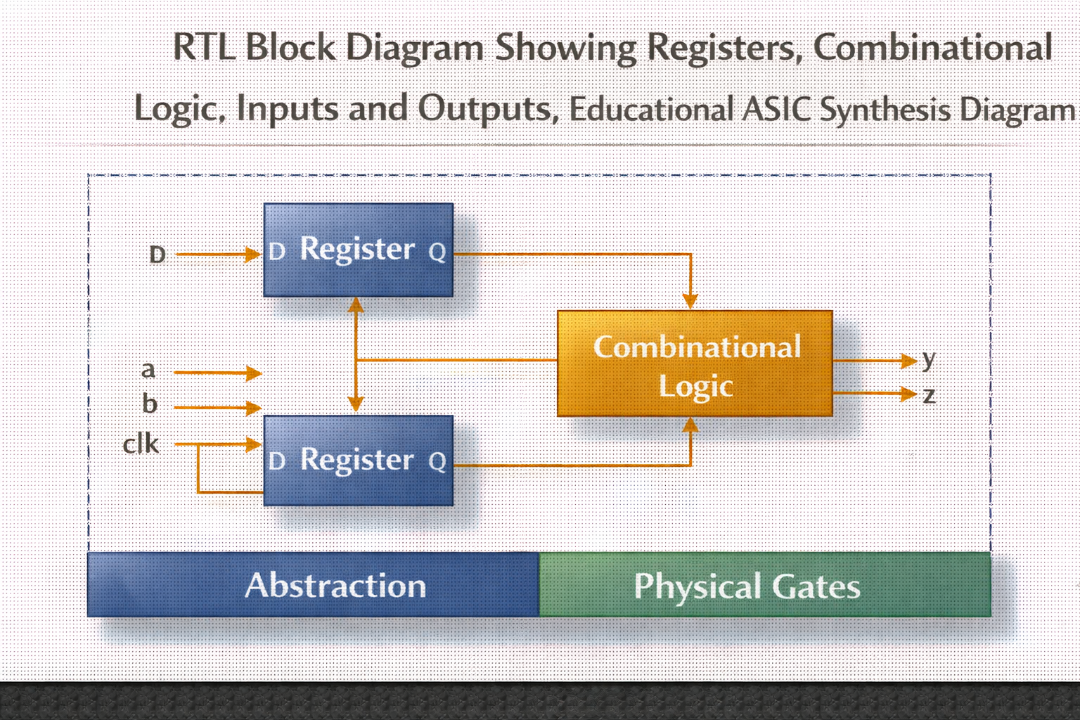
2. Input-1: RTL (Register Transfer Level)
What is RTL input?
RTL is the functional description of the design written in:
- Verilog
- SystemVerilog
- VHDL
It tells: ✔ What logic to build ✔ How data flows ✔ When registers capture data
Example RTL:
module and_gate (
input a, b,
output y
);
assign y = a & b;
endmodule
What information RTL provides?
RTL Contains | RTL Does NOT Contain |
Logic behavior | Gate delays |
Registers | Cell sizes |
Control logic | Power info |
Functional correctness | Physical info |
Commands to read RTL (Synopsys DC example):
read_verilog design.v
or
analyze -format verilog design.v
elaborate top_module
3. Input-2: Technology Library (.lib)
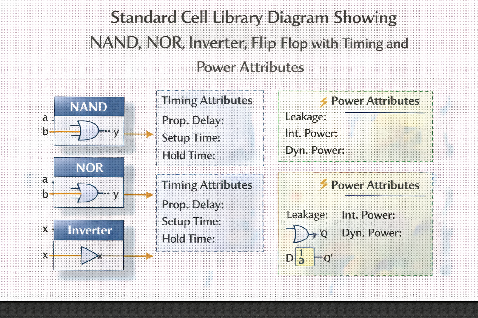
What is .lib file?
lib describes ALL standard cells available in the technology.
It is provided by:
- Foundry (TSMC, Samsung, Intel)
- Or standard cell vendor
What .lib contains (CRITICAL):
Parameter | Meaning |
Cell name | NAND2_X1, DFF_X2 |
Area | Cell size |
Delay | Timing arcs |
Power | Leakage & dynamic |
Drive strength | X1, X2, X4 |
Setup/Hold | Flip-flop timing |
Example Cell in .lib:
cell (NAND2_X1) {
area : 1.23;
pin (Y) {
timing() {
related_pin : "A";
cell_rise : 0.12;
}
}
}
Why .lib is mandatory?
Without .lib: Tool doesn’t know what gates exist Cannot calculate timing Cannot optimize
Synthesis becomes blind
Command to read library:
set target_library slow.lib
set link_library "* slow.lib"
4. Input-3: Timing Constraints (.sdc)
What is SDC?
SDC (Synopsys Design Constraints) tells the tool HOW FAST the design must run.
RTL says what to build SDC says how fast & how strict
What SDC defines:
Constraint | Purpose |
create_clock | Clock frequency |
set_input_delay | Input timing |
set_output_delay | Output timing |
set_false_path | Ignore paths |
set_multicycle_path | Multi-cycle logic |
Example SDC:
create_clock -name clk -period 10 [get_ports clk]
10ns period = 100 MHz
Input delay example:
set_input_delay 2 -clock clk [get_ports data_in]
Why SDC is required?
Without SDC: Tool doesn’t know performance target No timing optimization Wrong gate selection
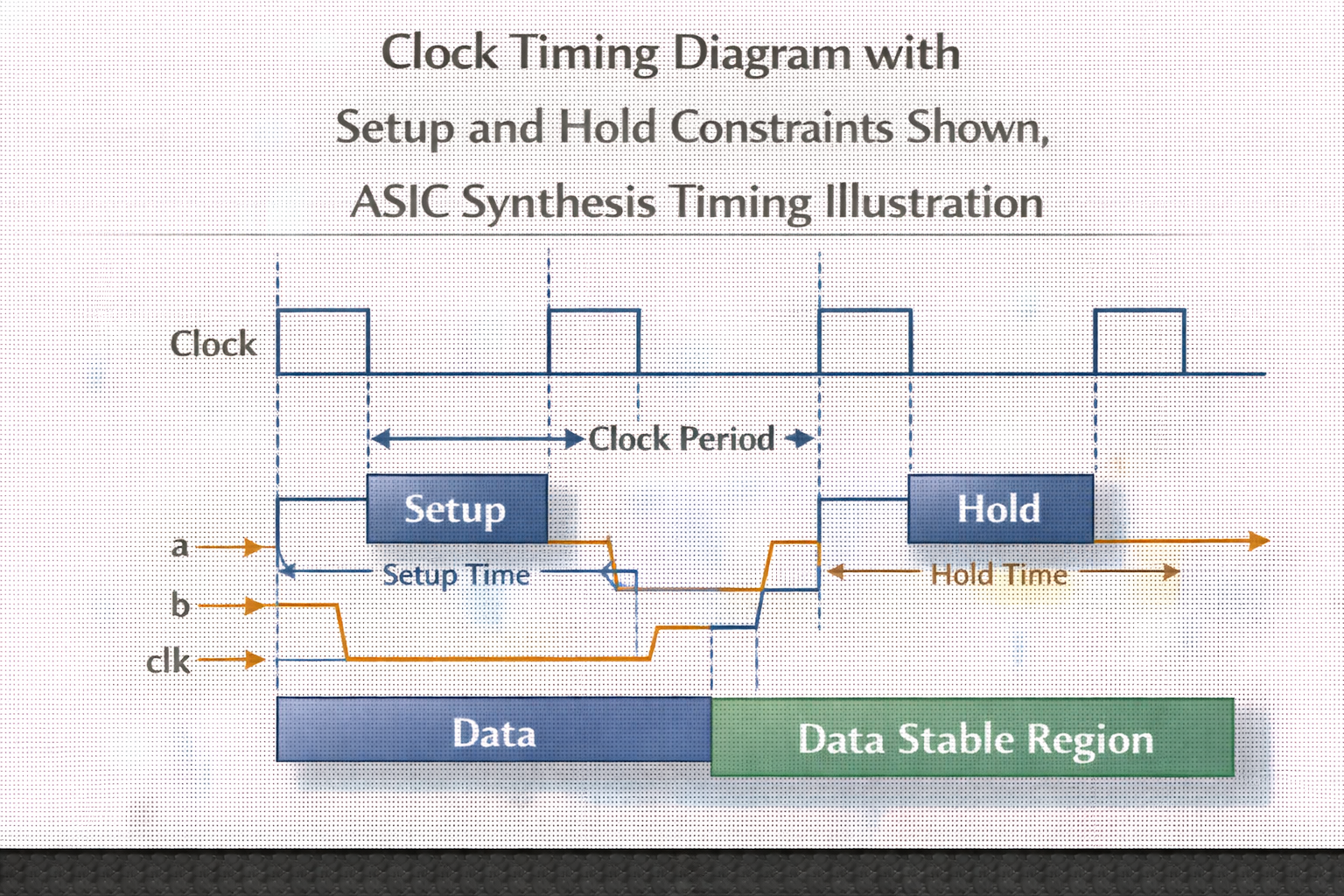
5. What Happens If Inputs Are Wrong?
Issue | Result |
Wrong RTL | Functional failure |
Wrong .lib | Timing mismatch |
Missing SDC | Over-design or under-design |
Tight SDC | Area & power increase |
Loose SDC | Timing failure later |
6. Complete Input Flow (Student Friendly)
RTL ─────┐
├──> LOGICAL SYNTHESIS ──> Gate Netlist
lib ─────┤
│
SDC ──────┘
7. Student Conclusion
✔ RTL = what to build ✔ .lib = what gates exist ✔ SDC = how fast it should run ✔ All three are MANDATORY
What Exactly Happens in Logical Synthesis – FLOW DIAGRAM EXPLANATION
1. First: Why a “flow diagram” is needed
Students often see this and feel confused:
RTL → Synthesis → Netlist
This is NOT sufficient
Logical synthesis internally has multiple transformation stages. If students don’t understand each block, they will fail in:
- Debugging timing
- Fixing synthesis errors
- Understanding reports
So now we go box by box, like an industry lecture.
2. Complete Logical Synthesis Flow (High-Level)
Here is the correct industry flow:
RTL Code
↓
RTL Analysis
↓
Elaboration
↓
Design Optimization
↓
Technology Mapping
↓
Constraint-Driven Optimization
↓
Gate-Level Netlist + Reports
Now we will open each box.
3. Block-1: RTL Code (Input Stage)
What is given to the tool?
- Verilog / SystemVerilog RTL
- Behavioral + structural code
- May contain:
- if / case
- always blocks
- arithmetic
- hierarchy
Example:
always @(posedge clk) begin
if (rst)
q <= 0;
else
q <= d;
end
At this stage:
- No gates
- No delays
- No power
- Just intent
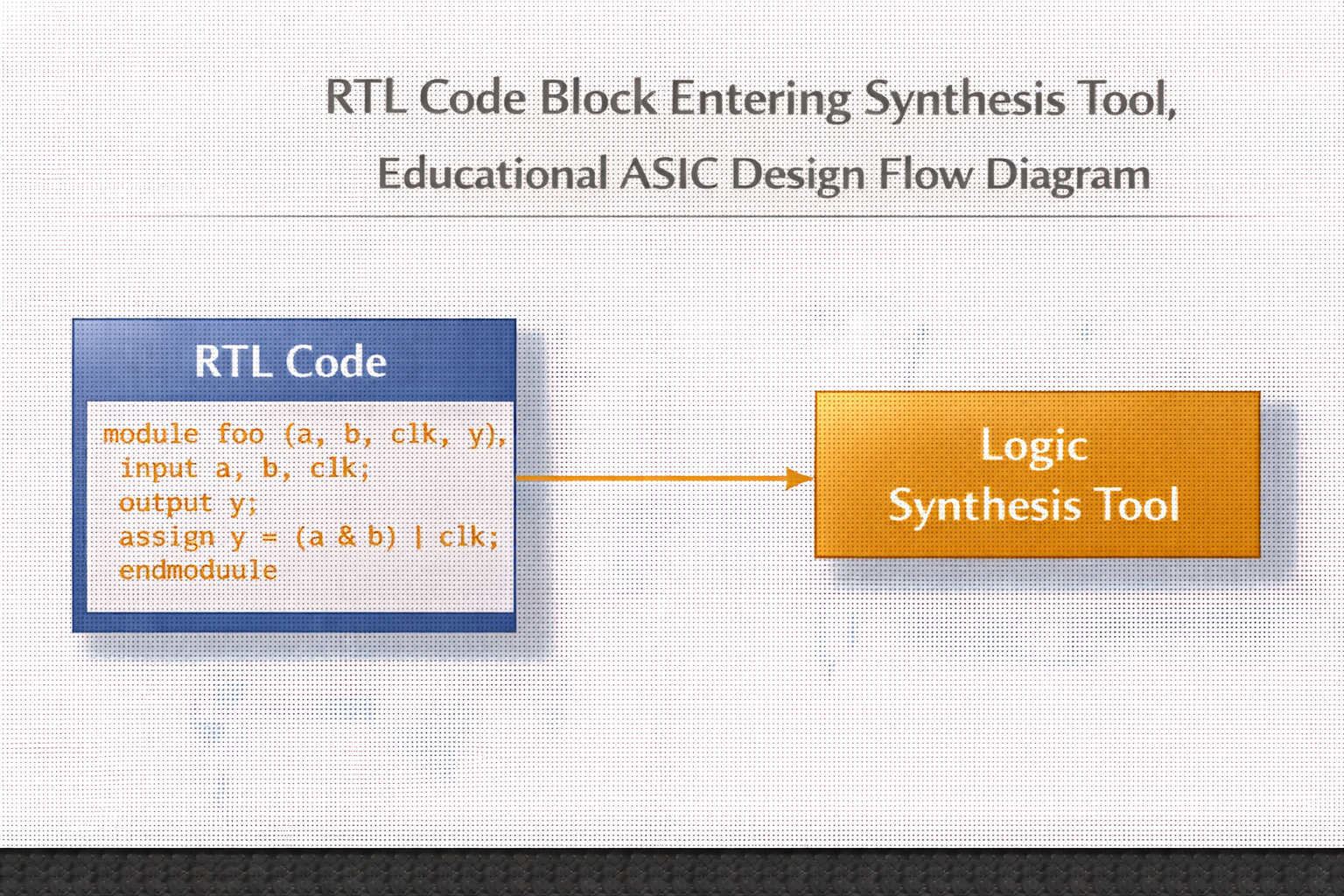
4. Block-2: RTL Analysis (Syntax + Semantic Check)
What happens internally?
The tool:
- Checks syntax correctness
- Checks signal directions
- Checks multiple drivers
- Checks width mismatches
Example error caught here:
assign y = a & b;
assign y = c | d; // multiple driver
Tool stops here if error exists
No hardware thinking yet
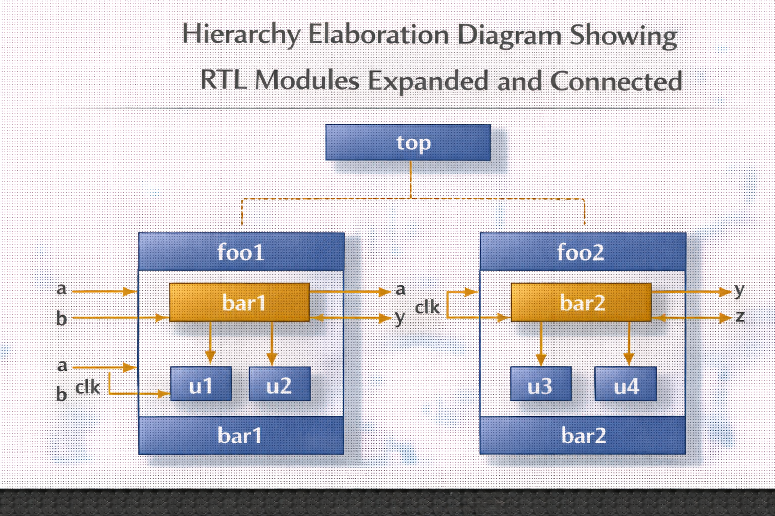
5. Block-3: Elaboration (Hierarchy Construction)
This is the MOST misunderstood stage
What elaboration really does:
- Expands generate blocks
- Resolves parameters
- Connects all submodules
- Builds full design hierarchy
Before elaboration:
module top;
sub #(8) u1();
endmodule
After elaboration:
- Tool knows:
- sub width = 8
- internal nets
- exact connectivity
✔ Design becomes complete and concrete
6. Block-4: Generic Logic Creation (Abstract Logic)
Now tool converts behavior into generic logic
Example:
assign y = (a & b) | c;
Converted internally to:
AND → OR
Important:
- Still technology independent
- No NAND / NOR yet
- No delay
This is called generic netlist
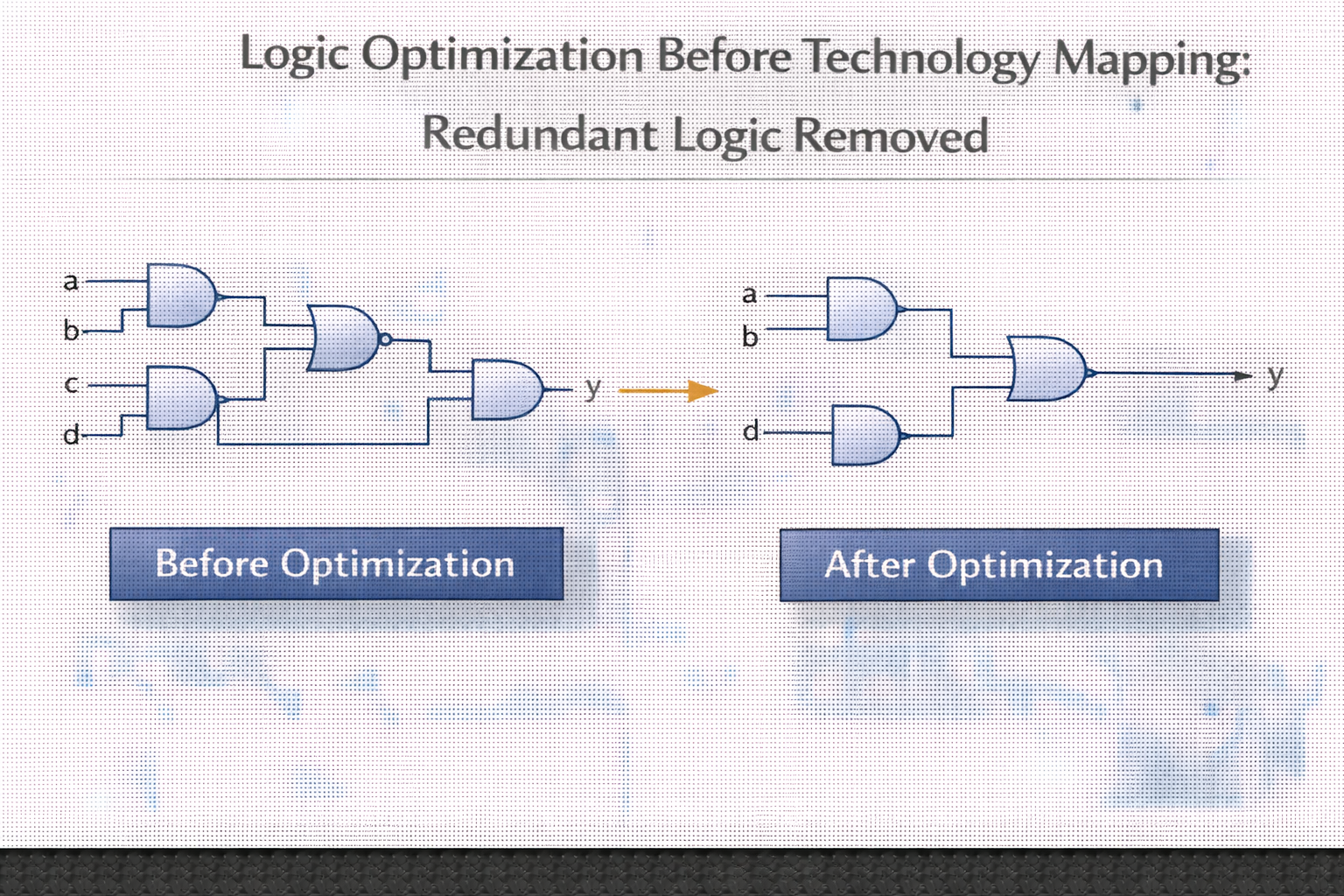
7. Block-5: Design Optimization (Pre-Mapping)
What optimization means here:
Improve logic without knowing real gates
Types of optimization here:
- Boolean simplification
- Constant propagation
- Dead logic removal
- Logic sharing
Example:
assign y = a & 1'b1;
Optimized to:
assign y = a;
✔ Function same ✔ Less logic
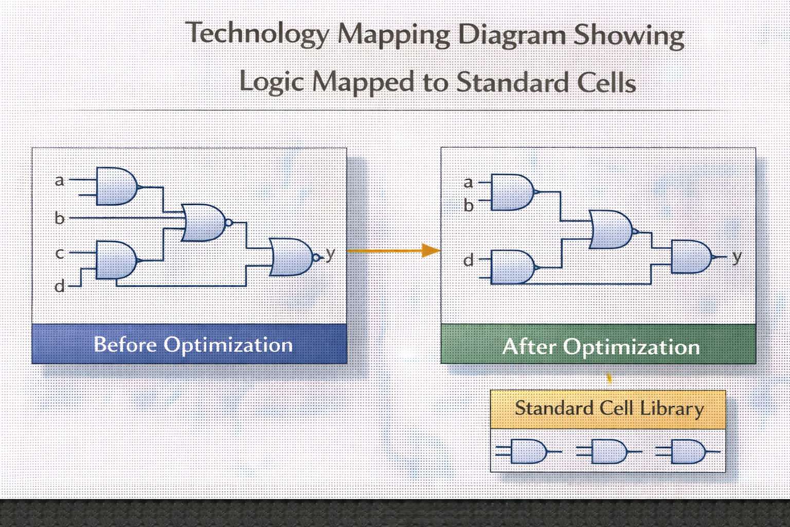
8. Block-6: Technology Mapping (Gate Selection)
Now tool asks:
“Which real cells can implement this logic?”
Tool looks into:
- .lib (standard cell library)
Generic logic:
AND
Mapped to:
AND2_X1
AND2_X2
AND2_X4
Tool selects based on:
- Timing
- Area
- Power
✔ Now design becomes real silicon logic
9. Block-7: Constraint-Driven Optimization (Post-Mapping)
Now SDC controls everything
Constraints like:
- Clock period
- Input delay
- Output delay
- Max area
Tool may:
- Upsize gates
- Restructure logic
- Replicate logic
- Balance paths
This loop may run many times.
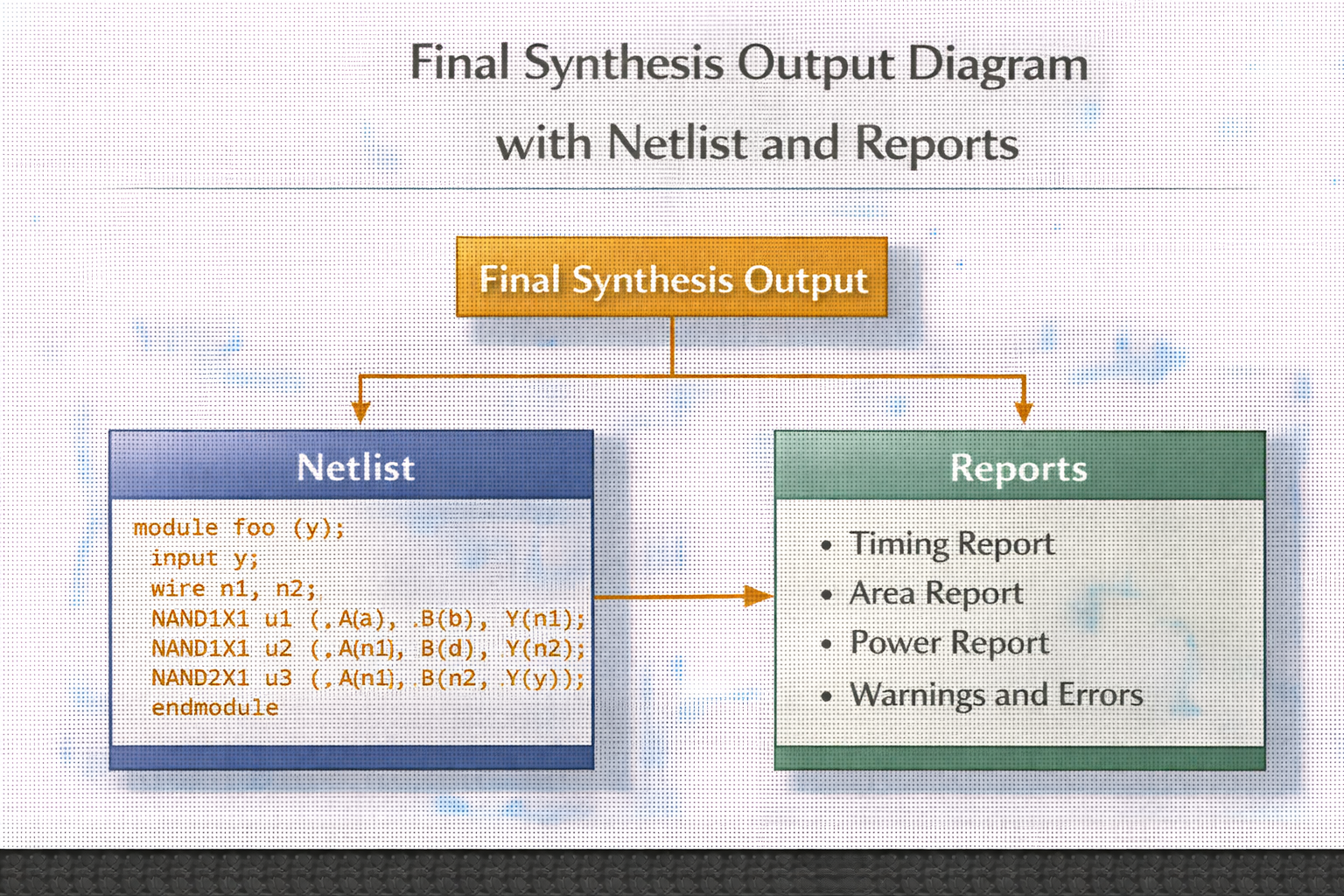
Block-8: Final Output Generation
Tool produces:
Main outputs:
- ✔ Gate-level netlist (.v)
- ✔ Timing reports
- ✔ Area reports
- ✔ Power reports
- ✔ Constraint files
Now design is:
- Ready for DFT
- Ready for PNR
1.1. Very Important Student Note
Logical synthesis flow is:
- RTL understanding → logic thinking → gate thinking
It is NOT:
- Coding tool
- Simulation tool
- Physical tool
1.2. Summary (Must remember)
- Flow has multiple internal stages
- Each stage modifies the design
- Errors at early stages affect everything later
- Understanding flow = strong VLSI foundation
CONCLUSION (Lecture Style)
Logical synthesis is not a black box. It is a step-by-step transformation engine that turns RTL intent into real gates under constraints.
Logical Synthesis – Advantages and Disadvantages (Industry Perspective)
This topic is very important for students, because interviewers often ask:
“Why do we need logical synthesis? What are its limitations?”
So we will not write bullet points only — we will explain WHY.
1. Why we even need Logical Synthesis (Context)
Before synthesis existed:
- Designers manually drew gates
- Huge designs → impossible to manage
- No automatic timing optimization
- Very high error rate
Logical synthesis solves this problem.
2. Advantages of Logical Synthesis (With Explanation)
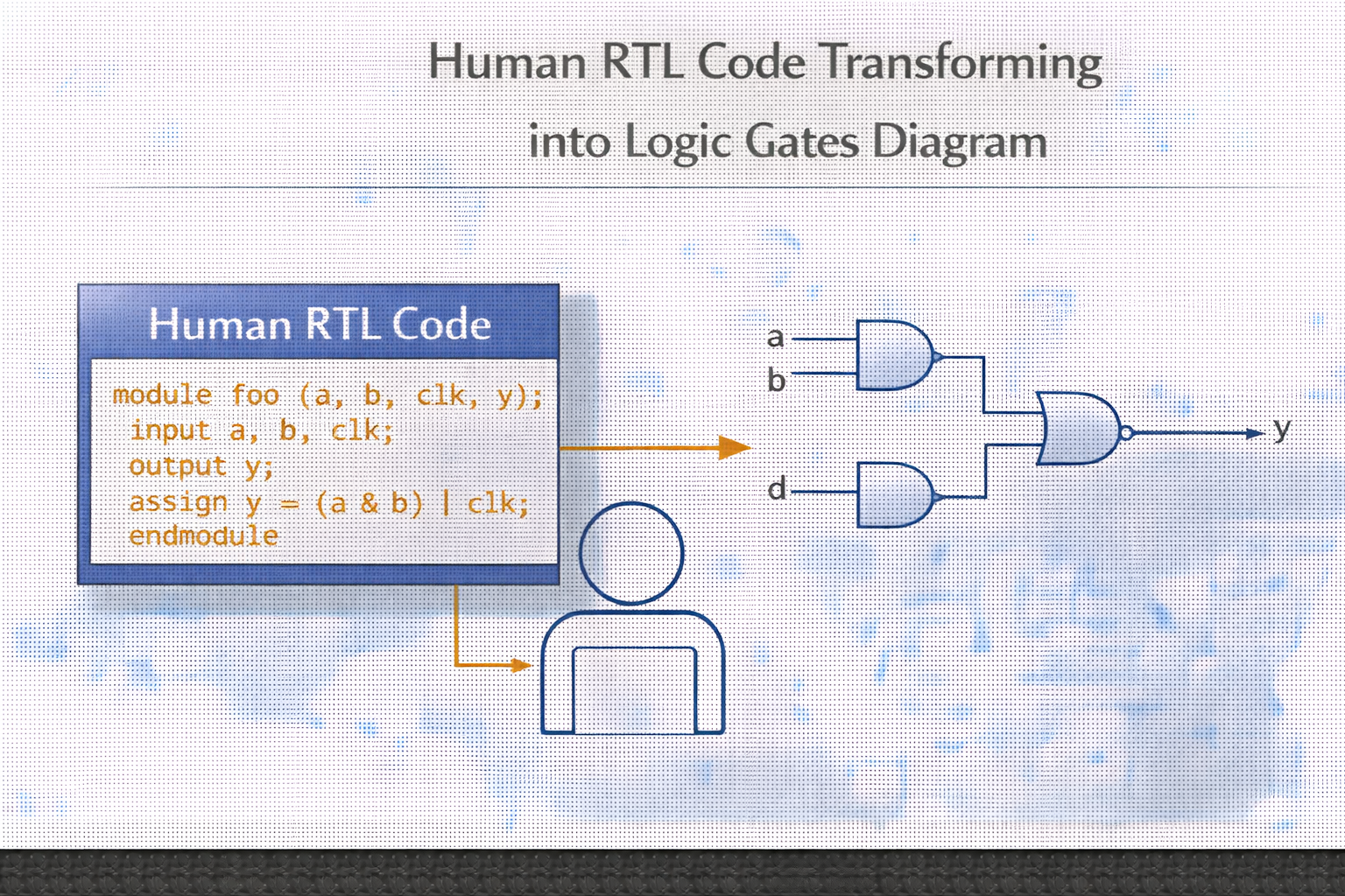
Advantage 1: Converts Human Intent into Hardware
RTL is human-readable:
if (a & b)
y = c;
else
y = d;
Logical synthesis:
- Understands logic meaning
- Converts it into gates automatically
✔ Designers focus on function, not gates ✔ Less human error
Advantage 2: Automatic Timing Optimization
Without synthesis:
- You don’t know gate delays
- You can’t fix timing
With synthesis:
- Tool knows:
- Cell delays
- Path delays
- Automatically:
- Restructures logic
- Upsizes gates
- Balances paths
Example:
- Slow AND → replaced by faster AND
- Logic depth reduced
✔ Meets clock frequency automatically
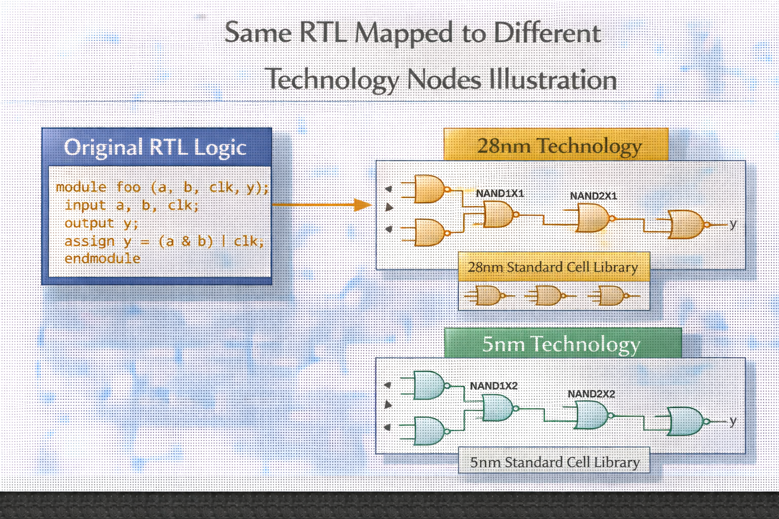
Advantage 3: Technology Independence
Same RTL can be used for:
- 28nm
- 14nm
- 7nm
Only .lib changes.
✔ RTL reusable ✔ Saves months of effort
Advantage 4: Area Optimization
Logical synthesis:
- Removes redundant logic
- Shares common logic
- Eliminates unused modules
Example:
assign y = a & b;
assign z = a & b;
Tool creates one AND gate, shares output.
✔ Smaller chip ✔ Lower cost
Advantage 5: Power Optimization
Power-aware synthesis:
- Chooses low-power cells
- Reduces switching activity
- Supports clock gating
✔ Lower dynamic power ✔ Better battery life
Advantage 6: Handles Huge Designs
Modern chips:
- Millions of gates
- Thousands of modules
Logical synthesis:
- Manages hierarchy
- Handles complexity automatically
✔ Impossible manually ✔ Industry-scale solution
3. Disadvantages of Logical Synthesis (Very Important)
Now the truth students must know.
Disadvantage 1: Depends Heavily on RTL Quality
Bad RTL ⇒ Bad netlist
Example:
always @(a or b or c or d or e or f)
Large sensitivity list Poor logic structure
Tool cannot fix bad architecture.
✔ Synthesis is NOT magic
Disadvantage 2: Limited Physical Awareness
Logical synthesis:
- Does NOT know real placement
- Does NOT know wire congestion
- Does NOT know routing delay accurately
Result:
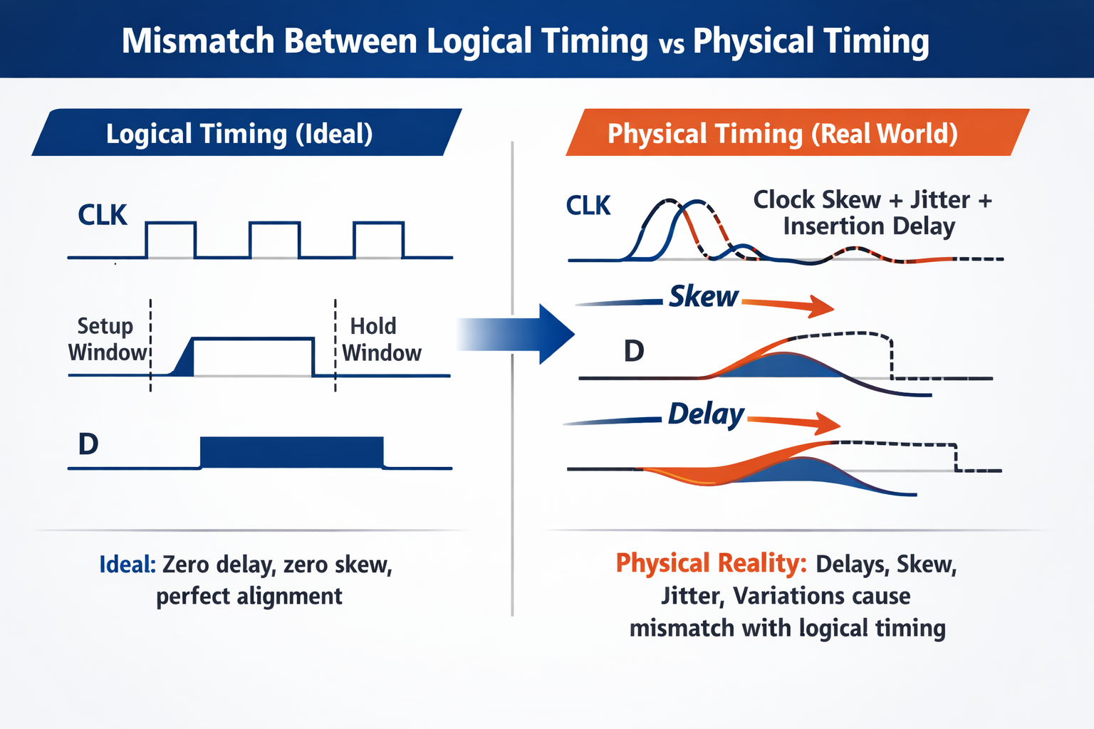
- Timing looks good in synthesis
- Fails in PNR
✔ Needs physical synthesis later
Disadvantage 3: Over-Optimization Risk
Aggressive constraints:
- Very tight clock
- Very low area limit
Tool may:
- Insert too many buffers
- Replicate logic excessively
Result:
- Higher power
- Hard-to-route design
Disadvantage 4: Tool-Dependent Results
Same RTL + different tools:
- Different netlists
- Different timing
- Different area
✔ Designer must understand tool behavior
Disadvantage 5: Debug Complexity
After synthesis:
- Gate-level netlist is hard to read
- Debugging becomes difficult
RTL:
if (a) y = b;
Gate-level:
U123 NAND2_X1
U124 INV_X2
..
✔ Debugging needs experience
4. When Logical Synthesis is NOT Enough
Logical synthesis cannot handle:
- Congestion
- IR drop
- Crosstalk
- Real wire delay
That is why: Physical synthesis exists
5. Industry Reality (Very Important)
Stage | Role |
RTL | Function correctness |
Logical Synthesis | Logic optimization |
Physical Synthesis | Physical realism |
PNR | Final silicon |
Skipping logical synthesis is impossible Over-trusting logical synthesis is dangerous
6. Student-Friendly Summary
Advantages:
- Automates gate creation
- Optimizes timing, area, power
- Technology independent
- Handles large designs
Disadvantages:
- RTL quality matters
- Limited physical awareness
- Tool-dependent
- Debug is hard
7. Final Conclusion (Lecture Style)
Logical synthesis is the brain of the ASIC flow. It understands intent, optimizes logic, and prepares the design for physical reality — but it cannot replace good RTL or physical design knowledge.
Combinational Merging & Sequential Merging in Logical Synthesis
This topic is very important because:
- It directly affects area, timing, and power
- Many students see this in reports but don’t understand WHY it happens
We will explain slowly, from basics, with examples.
1. First Understand: What is “Merging”?
Merging means:
The synthesis tool combines similar or duplicate logic into a single logic block to optimize the design.
Why?
- Reduce area
- Reduce redundant logic
- Improve power
There are two types:
- Combinational Merging
- Sequential Merging
2. Combinational Merging (In Depth)
What is Combinational Logic?
Combinational logic:
- Output depends only on current inputs
- No memory
Examples:
- AND, OR, MUX, ADDER
What is Combinational Merging?
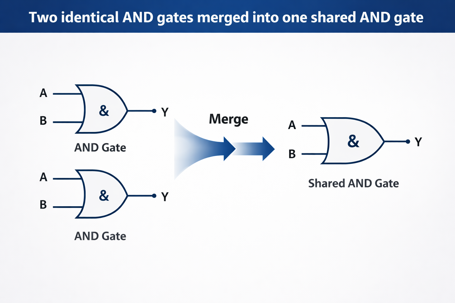
If the tool finds identical combinational logic, it:
- Keeps one copy
- Shares it across multiple outputs
Simple RTL Example
assign y1 = a & b;
assign y2 = a & b;
Without merging:
- Two AND gates created
With merging:
- One AND gate
- Output shared to y1 and y2
✔ Area reduced ✔ Power reduced
When Does Combinational Merging Happen?
Stage: ✔ During Optimization phase of Logical Synthesis
Flow:
RTL → Translation → Optimization → Mapping
↑
Combinational merging
More Realistic Example
assign t1 = (a & b) | c;
assign t2 = (a & b) | d;
Tool behavior:
- Extracts (a & b) as common logic
- Shares it
Why Tools Do Combinational Merging?
Benefit | Reason |
Area | Fewer gates |
Power | Less switching |
Timing | Reduced load sometimes |
When Combinational Merging is Dangerous
If logic is:
- On critical paths
- Drives different timing paths
Tool may avoid merging to meet timing.
3. Sequential Merging (In Depth)
What is Sequential Logic?
Sequential logic:
- Stores state
- Depends on clock
- Uses flip-flops / latches
What is Sequential Merging?
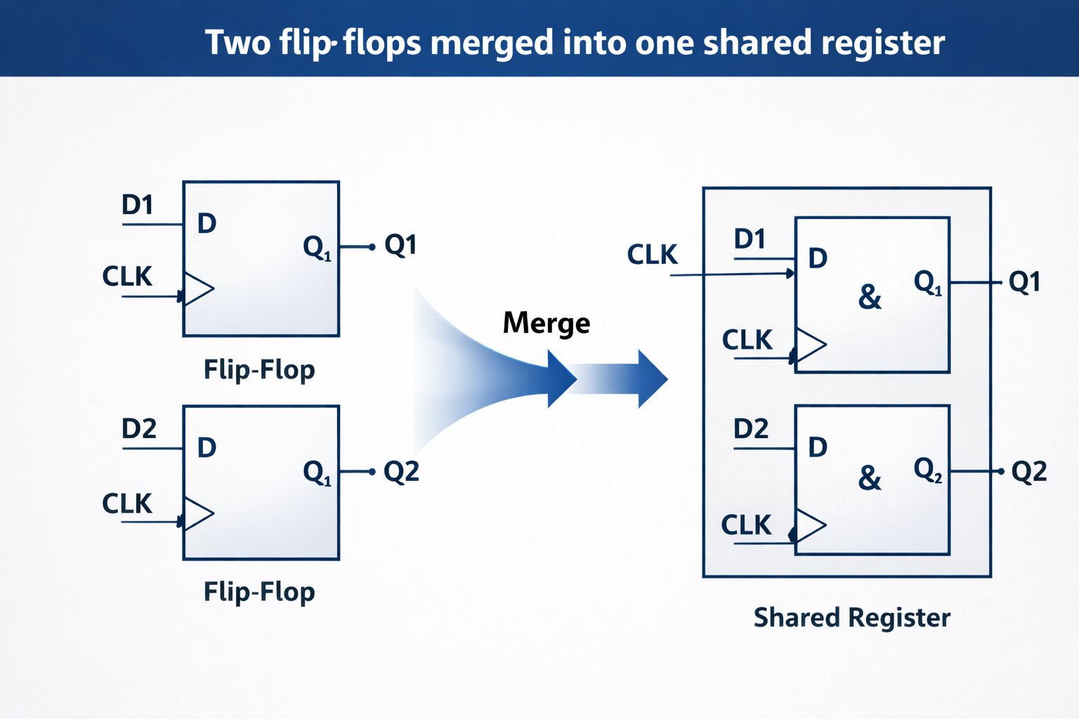
If multiple flip-flops:
- Have same clock
- Same reset
- Same data logic
- Same enable
Tool may:
- Merge them
- Reduce register count
RTL Example
always @(posedge clk)
q1 <= d;
always @(posedge clk)
q2 <= d;
Without merging:
- Two flip-flops
With merging:
- One flip-flop
- Output split
When Sequential Merging Happens?
Stage: ✔ During Optimization phase ✔ Before mapping
Why Sequential Merging is Risky
Sequential merging:
- Reduces registers
- But reduces flexibility
Problems:
- Harder timing fixes
- Harder ECOs
- Can break testability (DFT)
Because of this, sequential merging is often restricted.
4. How to Control Merging (Very Important)
Prevent Merging (Industry Usage)
set_dont_touch [get_cells reg1]
set_dont_touch_network [get_nets net1]
✔ Prevents both combinational & sequential merging
Why Engineers Prevent Merging?
- Critical path isolation
- Debug simplicity
- ECO friendliness
- DFT requirements
5. Combinational vs Sequential Merging (Comparison)
Feature | Combinational | Sequential |
Logic type | Gates | Flip-flops |
Risk | Low | High |
Area gain | Medium | High |
Timing impact | Usually good | Risky |
DFT impact | Low | High |
6. Interview-Level Understanding
Q: Does synthesis always merge logic? A: No. It depends on:
- Timing constraints
- Dont_touch constraints
- Design structure
7. Student Summary
- Merging = removing duplicate logic
- Happens in optimization phase
- Saves area and power
- Must be controlled carefully
8. Conclusion (Lecture Style)
Combinational merging is generally safe and beneficial, while sequential merging must be handled carefully because it affects timing, testability, and ECO flexibility.
Empty Module in Logical Synthesis – What it is, Why Tool Removes it
This topic confuses many beginners, so we’ll start from absolute ZERO.
1. What is a Module in RTL?
A module in Verilog:
- Is a block of hardware
- Contains logic (combinational or sequential)
- Has inputs, outputs, internal logic
Example:
module adder (
input a, b,
output sum
);
assign sum = a ^ b;
endmodule
✔ This module does something
2. What is an Empty Module?
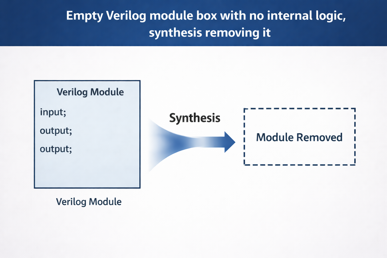
An empty module:
- Has no logic
- May have ports, but nothing inside
- Produces no hardware
Example of Empty Module
module empty_block (
input a,
output b
);
endmodule
No assign No always block No gates No registers
➡ This module does NOTHING
3. Why Do Empty Modules Exist?
Very important question
Common reasons:
1. Placeholder modules
- Used during early design
- Logic added later
2. Feature disabled by ifdef
`ifdef FEATURE_ON
assign y = a & b;
`endif
If FEATURE_ON is not defined → module becomes empty
3. Parameter-based removal
if (ENABLE == 0) begin
// no logic generated
end
4. IP integration shells
- Top-level created
- IP logic added later
4. What Does Synthesis Do with Empty Modules?
Synthesis Tool Behavior
If a module produces no hardware, the tool removes it
Because:
- It has zero gates
- It has zero effect
- Keeping it wastes nothing but confuses netlist
Synthesis Message Example
Warning: Removing empty module empty_block
This is NORMAL, not an error.
5. At Which Stage Empty Modules Are Removed?
Stage: ✔ Translation + Optimization
Flow:
RTL Read
→ Elaboration
→ Translation
→ Optimization ← empty modules removed
→ Mapping
6. Does Removing Empty Module Break Design?
NO, if:
- Module truly has no logic
- No outputs are used
✔ Safe removal
7. When Empty Module Removal is a PROBLEM?
Dangerous scenarios:
Case 1: Expected logic missing
- You thought logic exists
- But ifdef disabled it
Case 2: Missed macro definition
analyze -define FEATURE_ON
If missing → logic disappears
8. How to Detect Empty Modules Early?
Check Elaboration Report
elaborate top
check_design
Look for:
- “No logic inferred”
- “Empty module removed”
9. How to Prevent Removal (If Needed)?
Option 1. Add Dummy Logic (Rare)
wire dummy;
assign dummy = 1'b0;
Option 2. set_dont_touch (Not recommended for empty logic)
set_dont_touch [get_designs empty_block]
⚠ Tool may still remove if truly empty
Real Industry Example
In SoC projects:
- Many feature blocks are optional
- Disabled blocks → empty modules
- Tools automatically clean them
This is expected behavior
1.1. Interview Question
Q: Why synthesis removes empty modules? A: Because they generate no hardware and have no functional impact.
1.2. Student Summary
- Empty module = no logic
- Synthesis removes it automatically
- Happens during optimization
- Usually NOT an issue
- Sometimes indicates missing macro/parameter
1.3. Conclusion (Lecture Style)
Empty module removal is a cleanup process in logical synthesis to ensure only meaningful hardware is implemented in silicon.
set_dont_touch & set_dont_use – How to Control Synthesis Optimization
This is a VERY IMPORTANT topic in logical synthesis. Many real-time bugs happen because engineers don’t understand this properly.
1. Why Do We Need These Commands?
Reality of Logical Synthesis
Synthesis tool is intelligent. It tries to:
- Remove unused logic
- Merge logic
- Replace gates
- Optimize timing, power, area
But sometimes:
- You DON’T want optimization
- You want to protect logic
- You want to block certain cells
That is why set_dont_touch and set_dont_use exist.
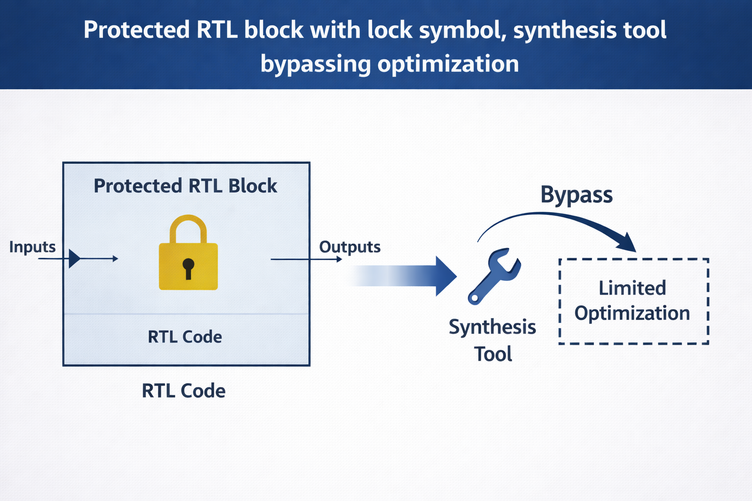
2. set_dont_touch – What Exactly It Does
Definition (Simple English)
set_dont_touch tells the synthesis tool: “DO NOT optimize, remove, or modify this object.”
What Can Be Protected?
You can protect:
- Module
- Cell
- Net
- Register
- Instance
Syntax
set_dont_touch <object>
Examples
Example 1. Protect a module
set_dont_touch [get_designs fifo_ctrl]
✔ Tool will:
- NOT remove
- NOT merge
- NOT restructure
Example 2. Protect a specific instance
set_dont_touch [get_cells u_clk_div]
Example 3. Protect a register
set_dont_touch [get_cells reg_*]
3. When Do We Use set_dont_touch? (Industry Cases)
Case 1: Debug logic
- Scan logic
- Observation logic
- Debug counters
Case 2: ECO-ready logic
- Logic kept for future fixes
Case 3: Pre-verified IP
- Don’t disturb proven logic
Case 4: Clock gating cells
- Must not be altered
4. set_dont_touch vs dont_touch_network
dont_touch_network
set_dont_touch_network [get_nets clk]
✔ Protects:
- Clock tree nets
- Reset nets
5. Important Warning (Very Important)
Overusing set_dont_touch is BAD
Why?
- Tool cannot optimize timing
- Area increases
- Power increases
- Timing violations may remain
Industry Rule
Use set_dont_touch only when absolutely required
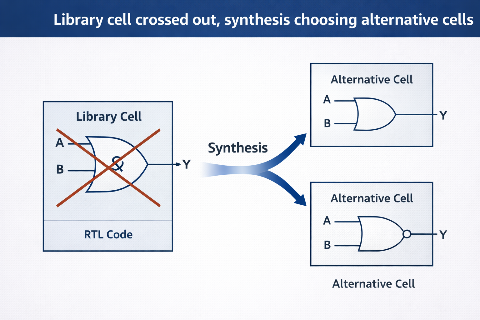
6. set_dont_use – What Exactly It Does
Definition
set_dont_use tells synthesis tool: “DO NOT use this library cell for mapping.”
Syntax
set_dont_use <lib_cell>
Example 1. Block a slow cell
set_dont_use [get_lib_cells */AND2_X1]
Example 2. Block low-VT cell (power reason)
set_dont_use [get_lib_cells */*_LVT]
7. Why set_dont_use is Needed?
Industry Reasons:
1. Timing risk
- Certain cells are slow
2. Power issue
- Some cells consume more leakage
3. DRC issue
- Foundry disallows some cells
4. Physical design constraints
- Cell causes congestion
8. Difference: set_dont_touch vs set_dont_use
Feature | set_dont_touch | set_dont_use |
Applied to | Design objects | Library cells |
Prevents | Optimization | Cell usage |
Used when | Logic must stay | Cell must not be used |
Stage | Optimization | Mapping |
9. Where These Commands Act in Synthesis Flow?
RTL
↓
Elaboration
↓
Translation
↓
Optimization ← set_dont_touch works
↓
Technology Mapping ← set_dont_use works
Real Industry Flow Example
read_verilog top.v
read_liberty slow.lib
set_dont_use [get_lib_cells */NAND2_X1]
set_dont_touch [get_cells u_scan_chain]
compile
✔ Scan logic preserved ✔ Bad cells avoided
1.1. Interview Questions
Q1: What happens if dont_touch is applied on large block? Timing closure becomes difficult
Q2: Can dont_touch prevent empty module removal? No, empty logic still removed
1.2. Student Summary
- set_dont_touch → protect logic
- set_dont_use → block cells
- Use carefully
- Overuse causes timing & area problems
1.3. Conclusion
These commands give control to synthesis engineer. Used wisely → design success Used blindly → timing failure
Unresolved References in Logical Synthesis
(One of the MOST COMMON & CONFUSING synthesis issues for beginners)
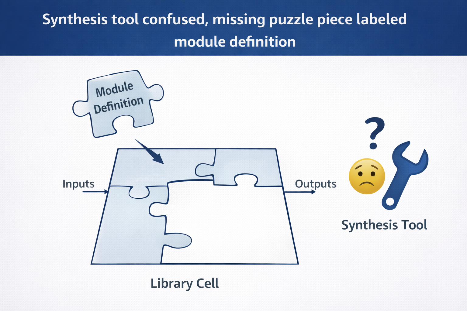
1. What is an Unresolved Reference?
Simple Definition (Student Friendly)
Unresolved reference means: Synthesis tool sees a module or cell name, but it does NOT know its definition.
In short:
- Tool knows the name
- Tool does NOT know the implementation
Typical Error Message
Warning: Unresolved reference to module 'fifo_mem'
Warning: Unresolved reference to cell 'DFF_X1'
2. Where Does This Error Appear in Flow?
RTL Read
↓
Analyze
↓
Elaborate ← Unresolved reference detected HERE
↓
Translation
↓
Optimization
↓
Mapping
Important Unresolved reference is mainly caught during:
- analyze
- elaborate
3. Most Common Causes of Unresolved References
1. Missing RTL File
module top;
fifo u1(); // fifo.v not read
endmodule
✔ Tool error:
fifo module not found
2. Module Name Mismatch
module FIFO (...); // Capital letters
fifo u1 (...); // lowercase
Verilog is case-sensitive
3. Library Not Loaded (.lib)
DFF_X1 not found
Cause:
- Liberty file not read
- Wrong library
4. Black Box Module
module mem (...);
// no logic
endmodule
Tool treats it as:
- Black box
- No internal definition
5. Wrong Search Path
read_verilog ./rtl/top.v
But submodules are in:
/rtl/core/
4. Types of Unresolved References
Type 1: RTL Unresolved Reference
- Missing Verilog module
Type 2: Library Cell Unresolved Reference
- Missing standard cell (.lib)
Type 3: IP / Memory Black Box
- Expected in ASIC flow
5. How to Detect Unresolved References
Command
check_design
or
report_design_warnings
Output Example
Warning: Unresolved reference 'ram_32x8'
6. How to Fix Unresolved References (Step-by-Step)
Fix 1: Read All RTL Files
read_verilog rtl/*.v
✔ Best practice:
- Use wildcard
- Avoid missing files
Fix 2: Check Module Names
✔ Ensure:
- Same spelling
- Same case
- No typo
Fix 3: Load Correct Libraries
read_liberty slow.lib
read_liberty fast.lib
Fix 4: Set Search Path
set search_path "./rtl ./lib"
Fix 5: Use Black Box Intentionally
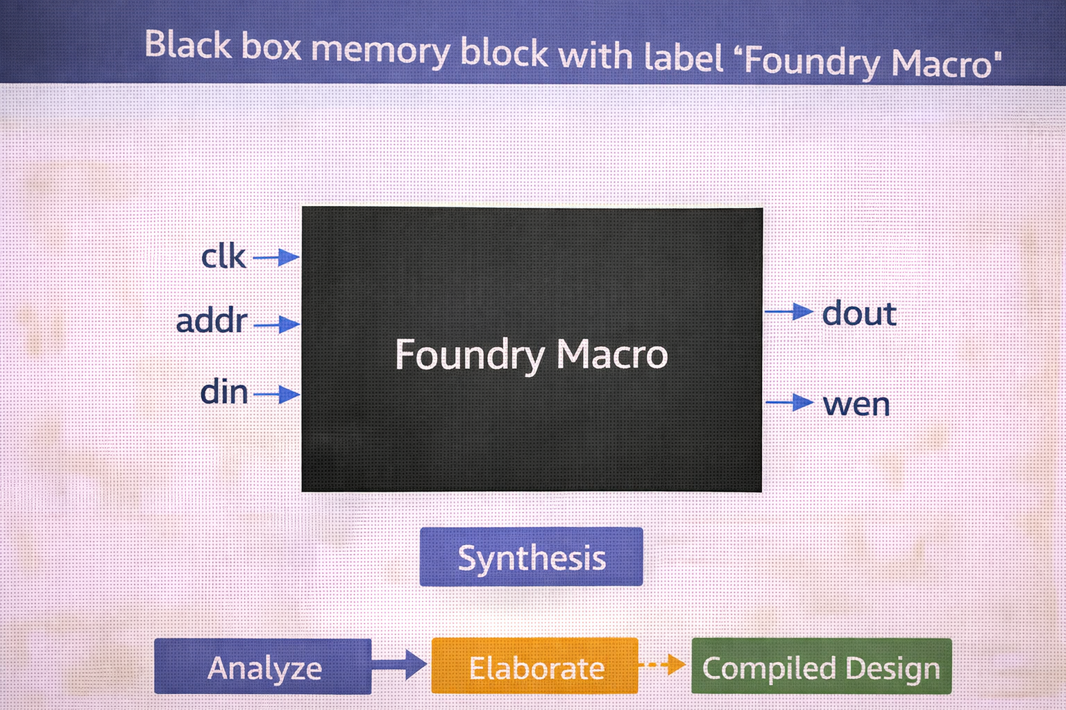
For memories:
set_black_box ram_32x8
Used when:
- Memory is replaced later
- Physical macro exists
7. Black Box vs Unresolved Reference
Aspect | Black Box | Unresolved |
Intentional | Yes | No |
Tool aware | Yes | No |
Error | No | Yes |
Used for | Memories, IPs | Mistakes |
8. Real Industry Example
Scenario:
- SRAM provided by foundry
- RTL model not given
Solution:
set_black_box SRAM_1Kx32
✔ Synthesis continues ✔ Timing abstracted
9. What Happens If You Ignore It?
Tool may:
- Remove logic
- Create floating nets
- Produce incorrect netlist
- Cause PNR failure
NEVER ignore unresolved references
Interview Questions
Q1: Can synthesis proceed with unresolved references? No (except black boxes)
Q2: Are unresolved references allowed in PNR? No
1.1. Student Summary
- Unresolved reference = missing definition
- Happens during analyze/elaborate
- Caused by missing RTL or library
- Fixed by reading files or black boxing
1.2. Conclusion
Unresolved reference is not a tool bug. It is a design completeness problem. A good synthesis engineer fixes it before compile.
Clock Gating in Logical Synthesis
(VERY IMPORTANT – asked in interviews + used in every real chip)
1. Why Clock Gating is Needed (Very Simple Start)
Problem First (Without Clock Gating)
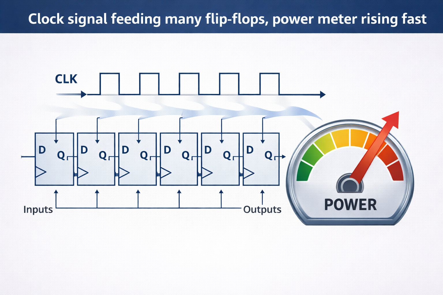
- Clock toggles every flip-flop
- Even when data is not changing
- Causes huge dynamic power waste
Fact
Clock network consumes 30–40% of total chip power
Real-Life Example
Think of:
- Ceiling fan running even when no one is in the room
➡ Waste of electricity ➡ Same happens with clock in IC
2. What is Clock Gating? (Correct Industry Definition)
Clock gating is a low-power technique where the clock signal is selectively turned OFF for idle registers, without affecting functionality.
In short:
- If data not changing → stop clock
- If data needed → allow clock
3. What Happens Without Clock Gating?
Aspect | Without Clock Gating |
Power | Very high |
Clock toggling | Always |
Battery life | Poor |
Thermal | High heat |
4. What Happens With Clock Gating?
Aspect | With Clock Gating |
Power | Reduced |
Clock toggling | Only when needed |
Performance | Same |
Area | Slight increase |
Important Clock gating affects power, NOT functionality.
5. Where Clock Gating is Added in Flow?
Correct Answer (Very Important)
RTL
↓
Analyze
↓
Elaborate
↓
Translation
↓
Optimization ← Clock Gating Inference HERE
↓
Mapping
Clock gating is added during OPTIMIZATION stage
6. Types of Clock Gating
1. RTL Clock Gating (Manual)
Example:
if (enable)
q <= d;
Tool infers:
- Enable-based gating
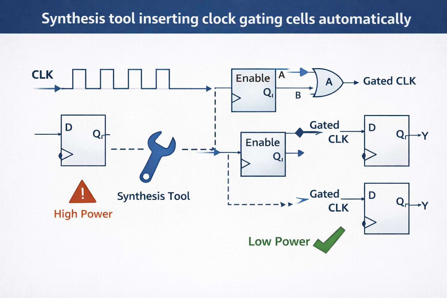
2. Synthesis Clock Gating (Automatic)
Tool inserts:
- Clock gating cells
- Based on data activity
✔ Most common in industry
7. Clock Gating Cell (Very Important)
What is a Clock Gating Cell?
A special standard cell containing:
- AND gate / Latch
- Glitch-free clock control
Why Normal AND Gate is NOT Used?
Causes:
- Clock glitches
- Timing failure
✔ Clock gating cell:
- Latch-based
- Safe for clock path
8. Clock Gating Working (Step-by-Step)
1. Enable = 0 → Clock blocked → Flops do NOT toggle
2. Enable = 1 → Clock passes → Flops toggle normally
9. Command to Enable Clock Gating (Industry Tool)
Synopsys DC Example
set_clock_gating_style \
-positive_edge_logic integrated \
-control_point before
Enable clock gating:
compile_ultra -gate_clock
Conditions for Clock Gating Inference
Tool checks:
- Enable condition
- Stable enable
- No async reset conflict
- Timing safe
If conditions fail → No gating
1.1. Example: RTL → Clock Gated Netlist
RTL Code
always @(posedge clk)
if (en)
q <= d;
Synthesized Result
CLK → CG_CELL → FF
↑
en
✔ Power saved ✔ Function same
1.2. Why Clock Gating is NOT Done in RTL Always?
Reason |
Hard to manage |
Clock tree issues |
Risk of glitches |
CTS complexity |
✔ Best practice:
Let synthesis insert gating
1.3. Advantages of Clock Gating
✔ Huge power reduction ✔ No performance loss ✔ Industry standard ✔ Essential for low-power chips
1.4. Disadvantages of Clock Gating
Extra area Slight timing complexity CTS becomes harder
1.5. Interview Questions
Q1: At which stage is clock gating added? Optimization stage
Q2: Why not use AND gate directly? Causes glitches
Q3: Does clock gating affect functionality? No
1.6. Student Summary
- Clock consumes most power
- Clock gating reduces dynamic power
- Inserted during synthesis optimization
- Uses special clock gating cells
1.7. Conclusion
Clock gating is the heart of low-power design. No modern chip exists without it.
How Timing is Met in Logical Synthesis
(MOST IMPORTANT for real projects & interviews)
1. First Understand: What is “Timing” in Synthesis?
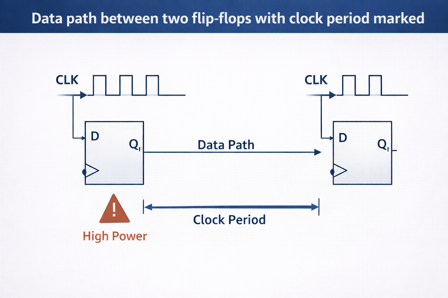
Simple Definition
Timing means data must travel from one register to another within the required clock period.
If it fails → Timing violation
Real-Life Example
Think of:
- Bus leaves at 10:00 AM
- Passenger must reach bus stop before 10:00
If late → missed bus Same in chip:
- Data must reach before clock edge
2. Types of Timing in Logical Synthesis
Type | Meaning |
Setup Timing | Data arrives before clock |
Hold Timing | Data stays stable after clock |
Max Delay | Long paths |
Min Delay | Short paths |
Logical synthesis mainly focuses on SETUP (Max delay)
3. Why Timing Fails After Synthesis?
Common reasons:
- Long combinational paths
- Too many logic levels
- Bad constraints
- Wrong hierarchy
- Over-optimized area
4. How Synthesis Tool Fixes Timing?
Tool uses multiple techniques, not just one.
Main techniques:
- Path grouping
- Ungrouping
- Boundary optimization
- Constraint tightening
- Cell resizing
- Logic restructuring
5. Path Grouping (group_path)
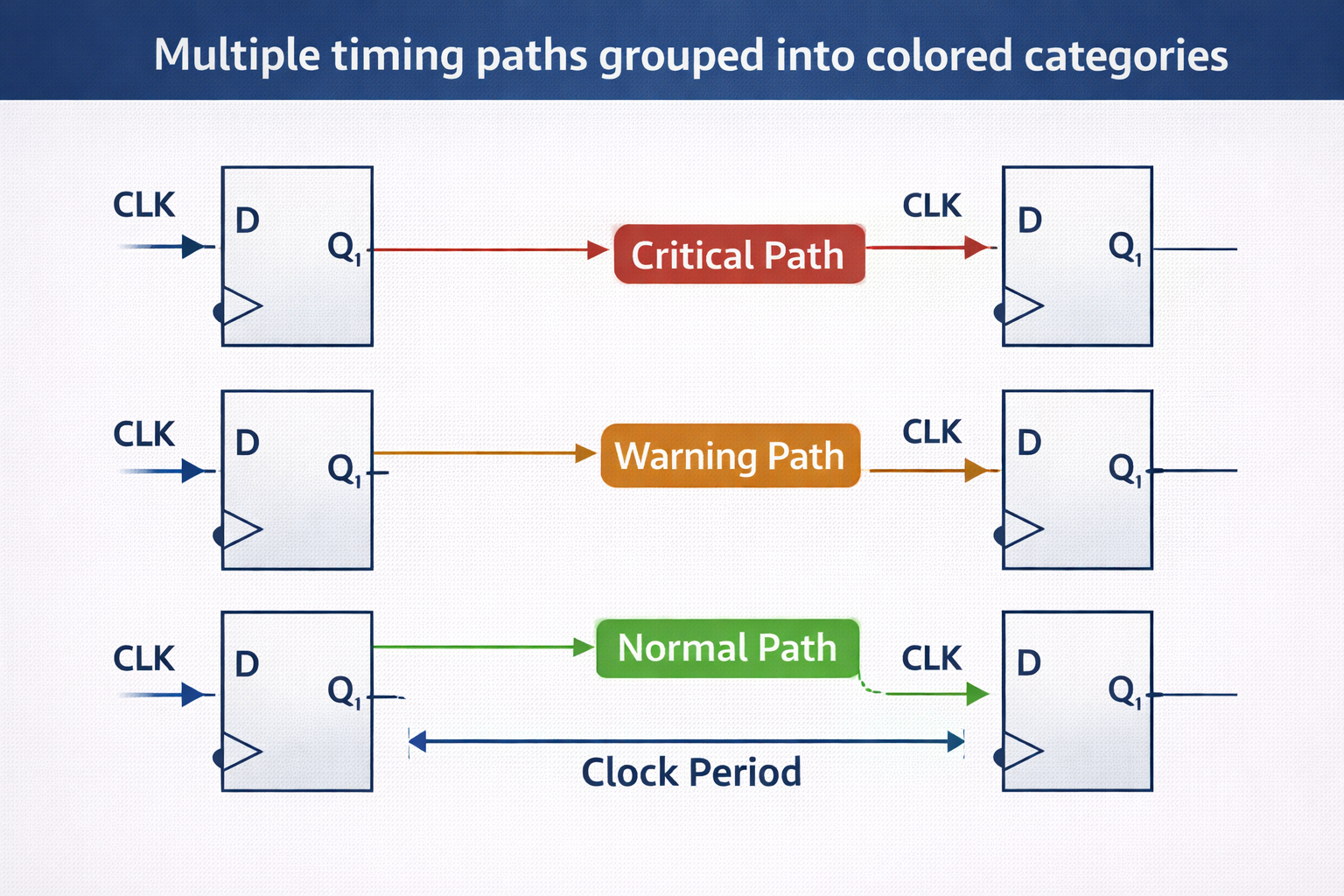
What is Path Grouping?
Dividing timing paths into meaningful groups so tool can optimize better.
Why Needed?
Without grouping:
- Tool treats all paths equally
- Critical paths may not get focus
With grouping:
- Critical paths optimized first
Example Path Groups
Group | Example |
reg2reg | Normal paths |
in2reg | Input to register |
reg2out | Register to output |
clk_gating | Clock gating paths |
Command Example
group_path -name REG2REG -from [all_registers] -to [all_registers]
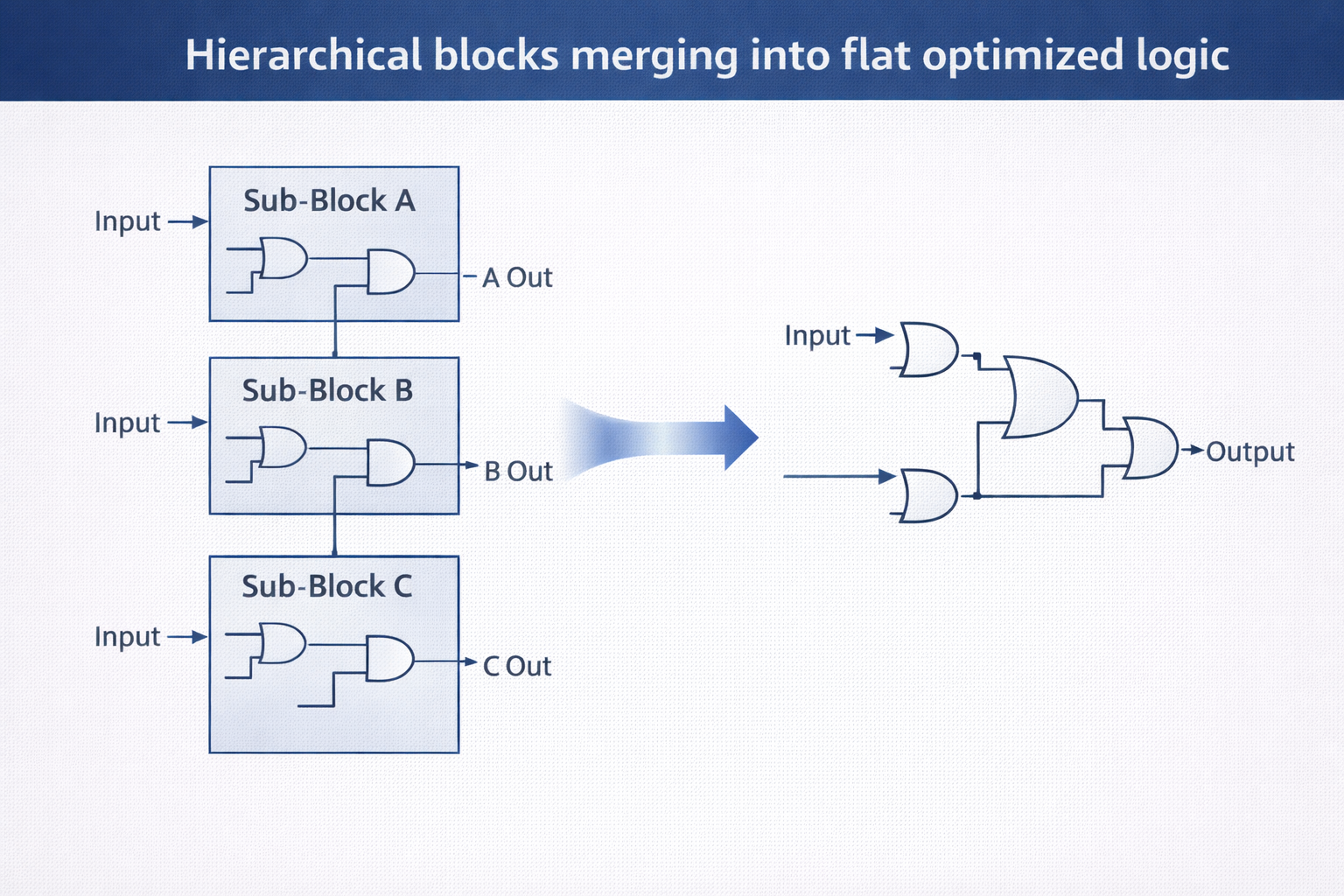
6. Ungrouping (Hierarchy Flattening)
What is Ungrouping?
Removing hierarchy boundaries so synthesis can optimize across modules.
Why Needed?
Hierarchy blocks:
- Logic sharing
- Gate restructuring
- Optimization across modules
Example
Without ungrouping:
Module A → Module B
With ungrouping:
Flat logic → optimized globally
Command
ungroup -all -flatten
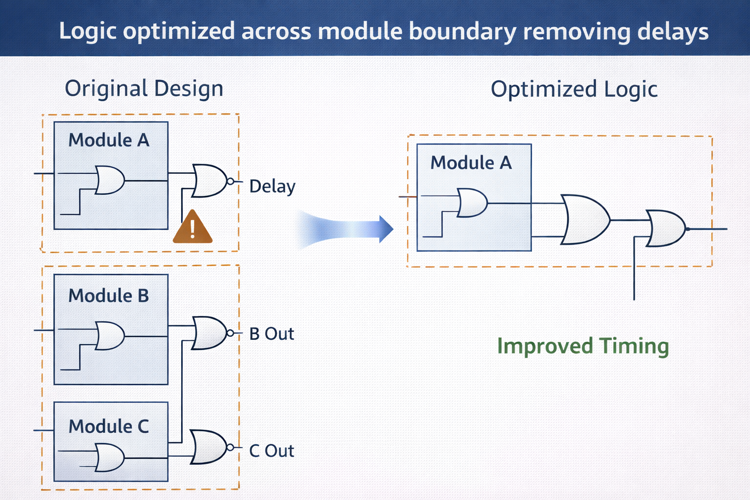
7. Boundary Optimization
What is Boundary Optimization?
Optimizing logic across module boundaries to reduce delay.
Why Important?
- Registers at boundaries
- Long combinational logic split badly
- Timing violations occur at module edges
Command
set_boundary_optimization true
8. Constraint Tightening
What is Constraint Tightening?
Intentionally giving tighter timing constraints to force aggressive optimization.
Example
Actual clock:
10 ns
Given constraint:
8 ns
Tool works harder → better timing margin
Command
create_clock -period 8 [get_ports clk]
9. Cell Resizing & Logic Restructuring
Tool automatically:
- Uses faster cells
- Increases drive strength
- Reduces logic depth
- Balances paths
Example:
NAND → AOI → OAI
Multi-Corner Multi-Mode (MCMM)
Tool optimizes for:
- Different clocks
- Different modes
- Different corners
Ensures timing closure in real silicon
1.1. Timing Closure Strategy (Industry)
1. Clean constraints 2. Group paths 3. Fix hierarchy 4. Optimize critical paths 5. Re-run compile 6. Check reports
1.2. Commands Used for Timing
report_timing
report_constraint
report_qor
1.3. Advantages of These Techniques
✔ Better timing ✔ Fewer ECOs later ✔ Cleaner PNR handoff
1.4. Disadvantages / Cautions
Too much flattening increases area Over-tight constraints increase power Poor grouping hides real critical paths
1.5. Interview Questions
Q: What is grouping vs ungrouping? Grouping = path focus Ungrouping = hierarchy removal
Q: Why tighten constraints? Force better optimization
1.6. Student Summary
- Timing is main goal of synthesis
- Tool uses multiple optimization tricks
- Engineer guides tool using constraints & commands
1.7. Conclusion
Timing closure is not automatic. Good synthesis engineer = good constraint writer.
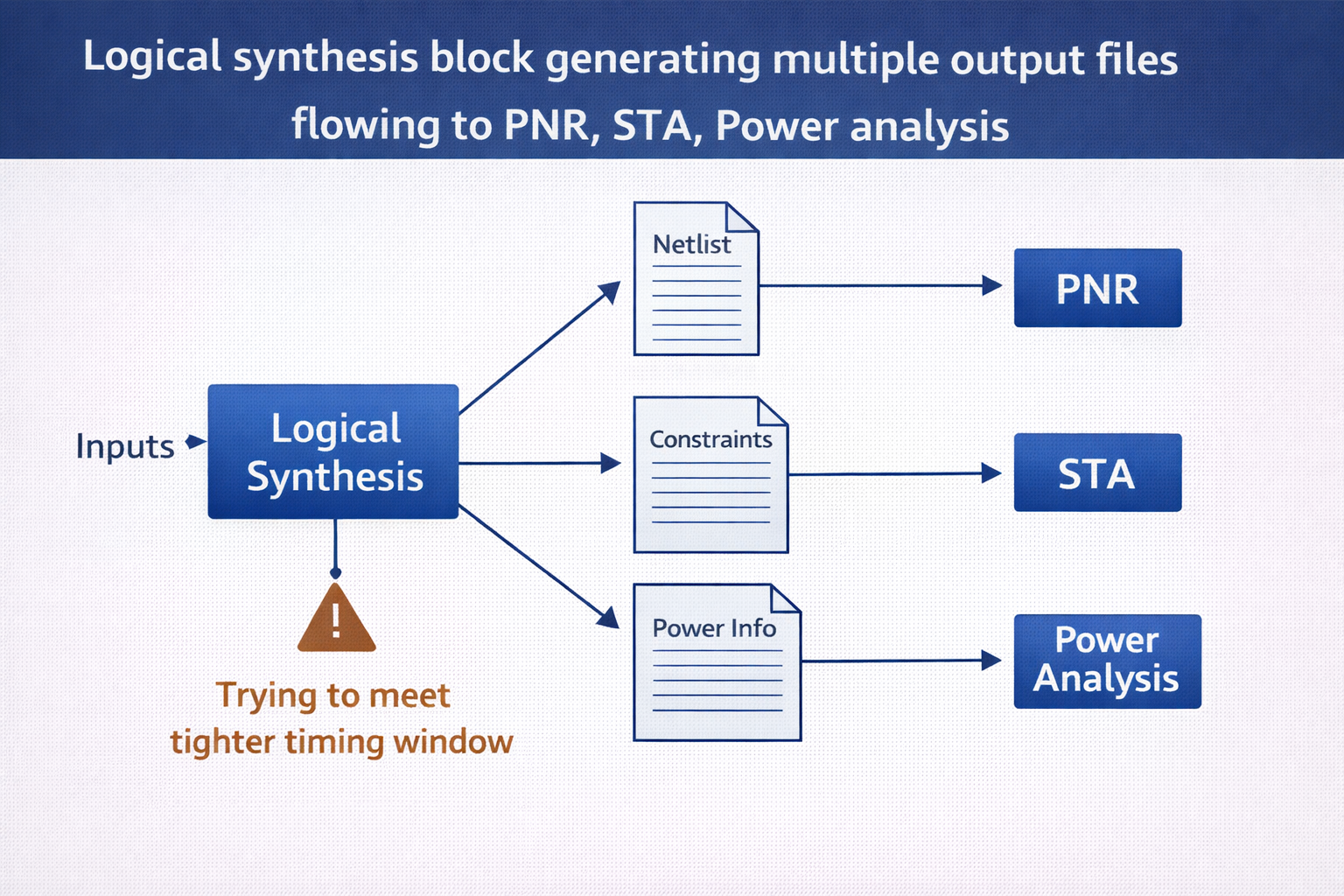
Outputs of Logical Synthesis (Industry Perspective)
After logical synthesis completes, tools do NOT just give one file. They generate multiple critical outputs that are used by PNR, STA, DFT, Power teams.
1. Why Outputs of Logical Synthesis Are Important?
Logical synthesis is NOT the end. It is a handoff stage.
Outputs are used by:
- Physical Design (PNR)
- Static Timing Analysis (STA)
- Power Analysis
- ECO & Debug
- Tapeout checks
2. Main Outputs of Logical Synthesis
Output | Purpose |
Gate-level Netlist | Physical implementation |
SDC | Timing constraints |
DDC / DB | Tool internal database |
Timing Reports | Check timing |
Area Reports | Check area |
Power Reports | Check power |
QoR Reports | Overall quality |
We will explain each one deeply.
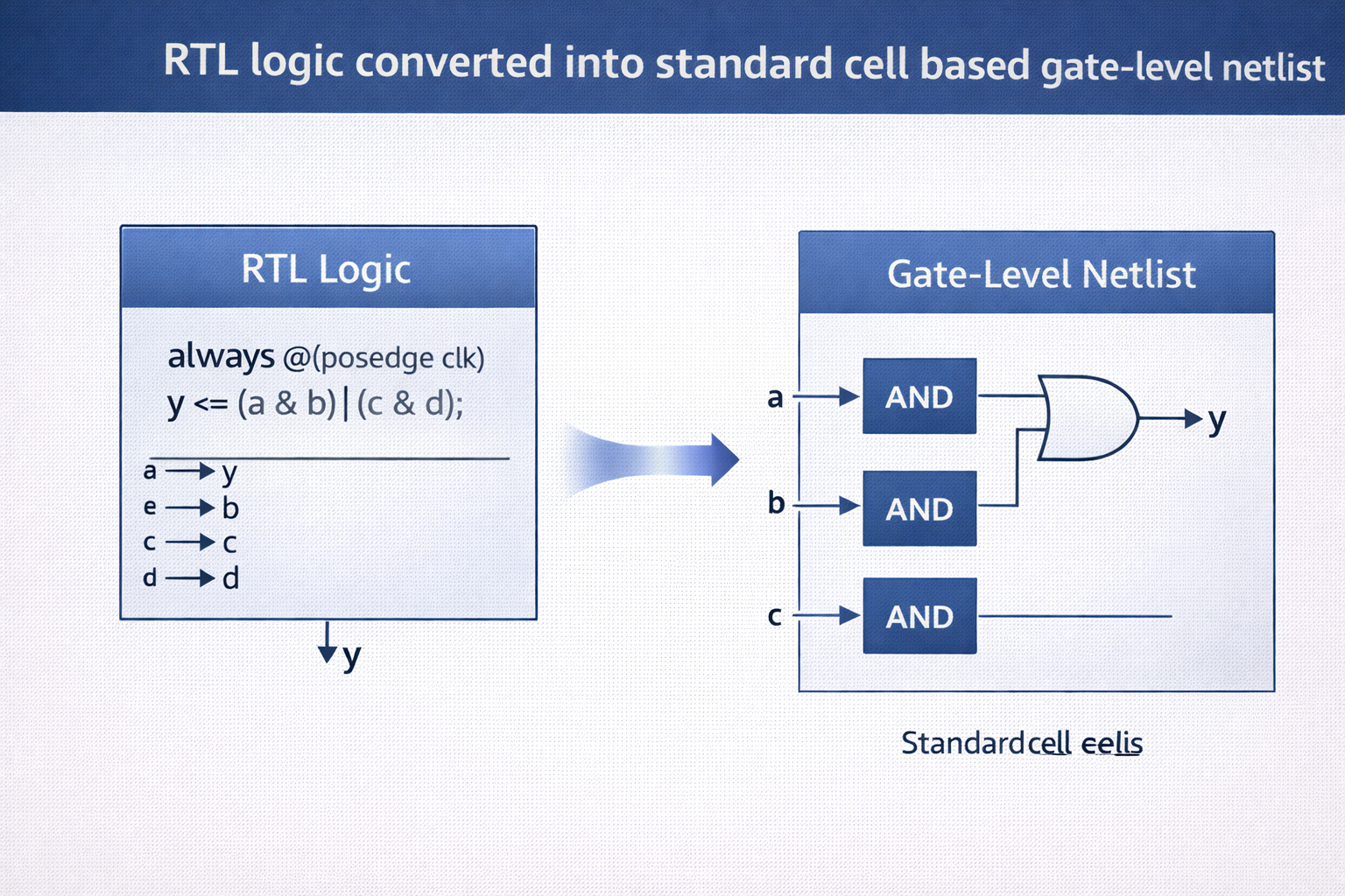
3. Gate-Level Netlist (.v)
What Is Gate-Level Netlist?
A Verilog file containing only standard cells from the technology library.
How It Looks
RTL (Before synthesis):
assign y = a & b;
Gate-level (After synthesis):
AND2_X1 U1 ( .A(a), .B(b), .Z(y) );
Why It Is Important
- Input for PNR
- Used for STA
- Used for GLS (Gate-level simulation)
Command to Generate
write -format verilog -hierarchy -output design_netlist.v
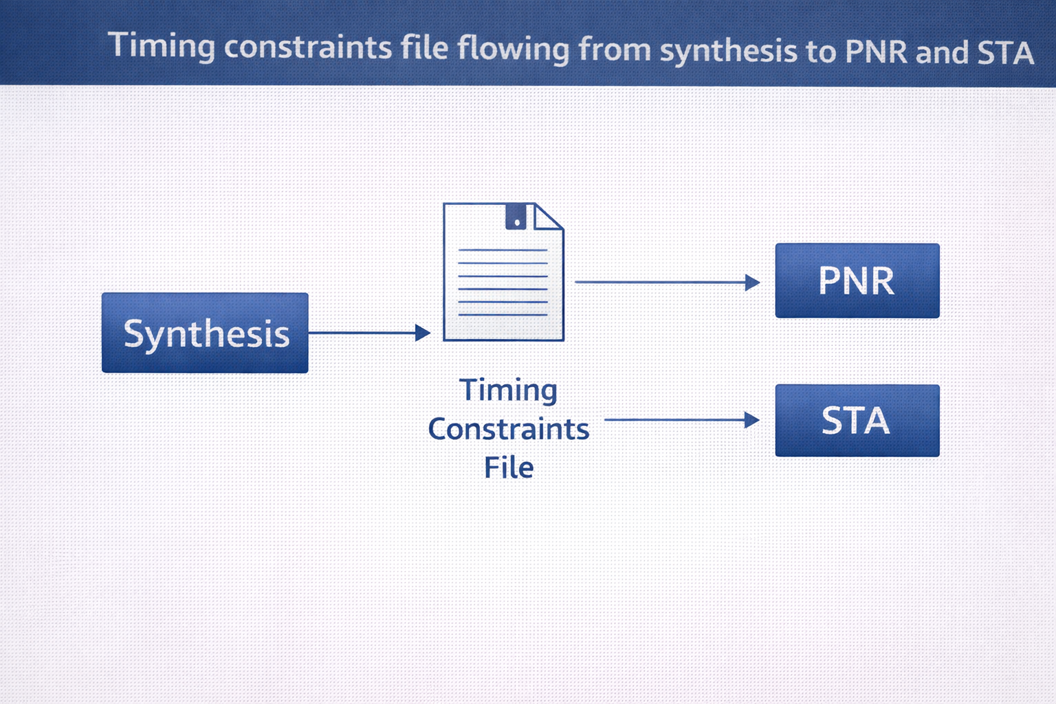
4. SDC (Synopsys Design Constraints)
What Is SDC?
A file that contains timing intent of the design.
Examples:
- Clock definition
- Input delays
- Output delays
- False paths
- Multicycle paths
Why Output SDC Is Needed?
- PNR must follow same timing intent
- STA must analyze using same constraints
Command to Write SDC
write_sdc design_constraints.sdc
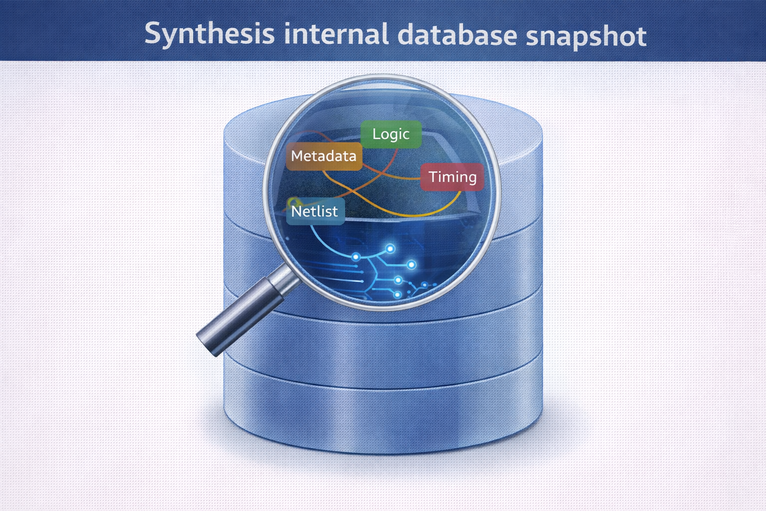
5. DDC / DB (Design Database)
What Is DDC?
Tool’s internal compiled database
Why Needed?
- Faster reload
- ECO friendly
- Preserves optimization history
Command
write -format ddc -hierarchy -output design.ddc
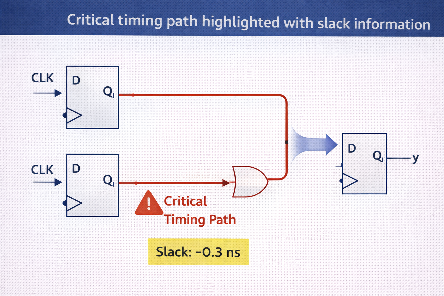
6. Timing Reports
Why Timing Reports?
To check:
- Setup violations
- Slack
- Critical paths
Command
report_timing
More detailed:
report_timing -max_paths 10 -delay_type max
Example Output Meaning
Term | Meaning |
Slack | Margin |
Negative slack | Timing failure |
Path | Critical logic |
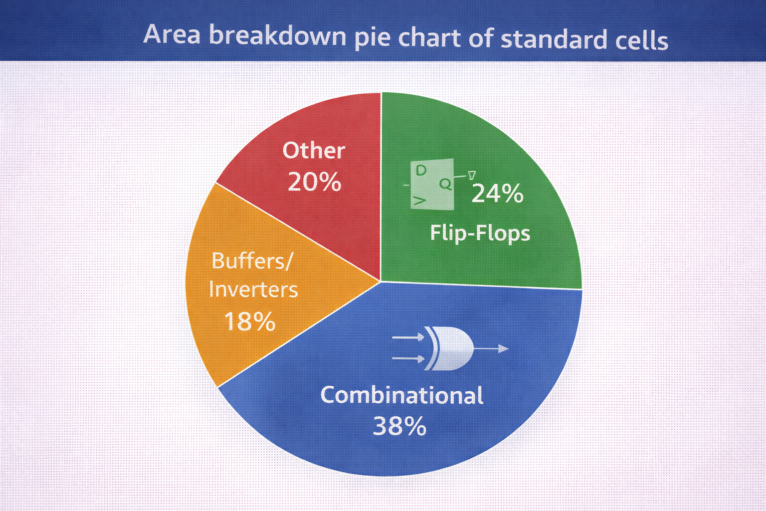
7. Area Reports
Why Area Reports?
- Check design size
- Compare optimization impact
- Cost estimation
Command
report_area
Example Information
- Total cell area
- Combinational vs sequential
- Hierarchy wise breakup
8. Power Reports
Why Power Reports?
- Power budget
- Battery life
- Thermal safety
Command
report_power
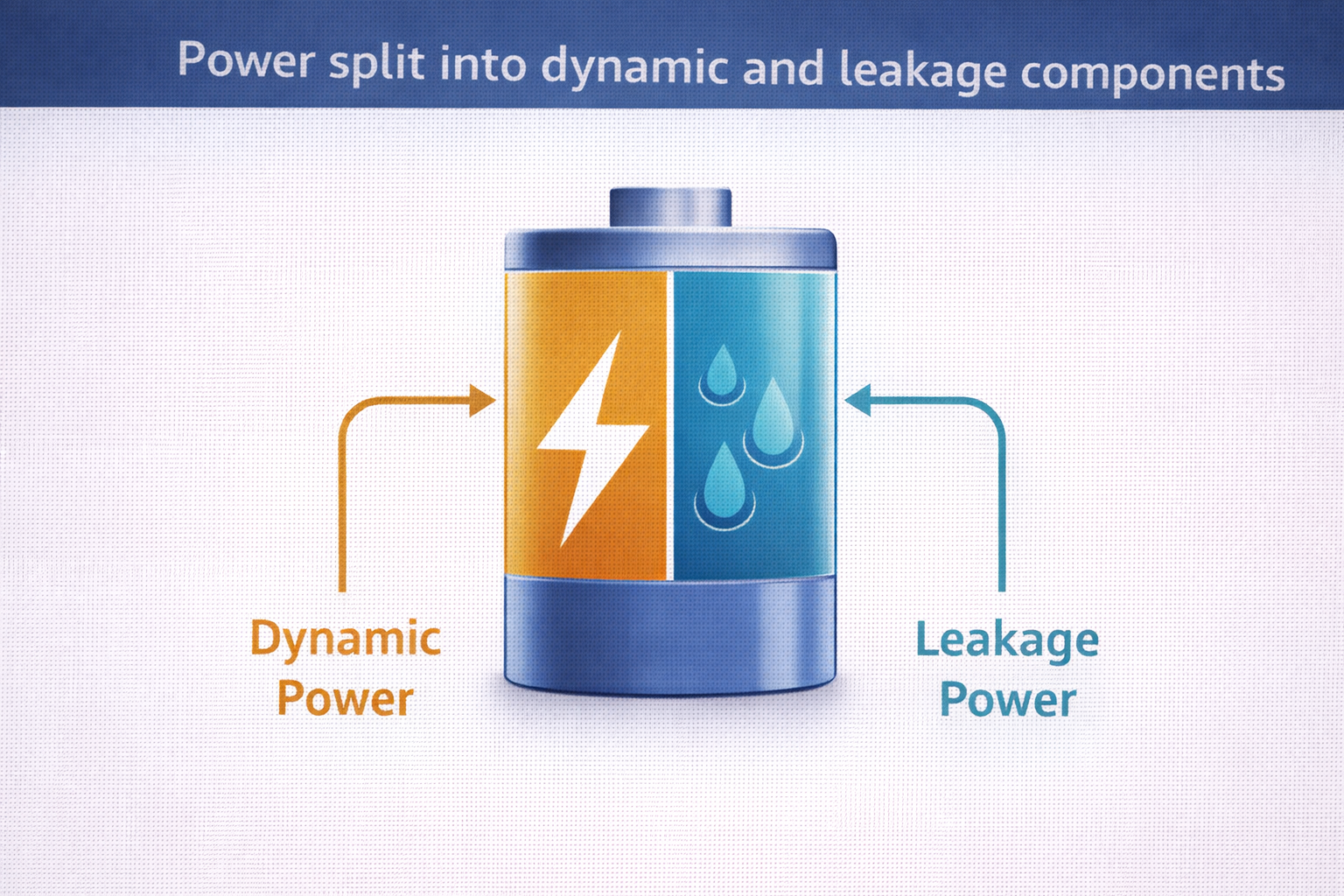
Types of Power
Type | Meaning |
Dynamic | Switching power |
Leakage | Static power |
Total | Overall power |
9. QoR (Quality of Results) Report
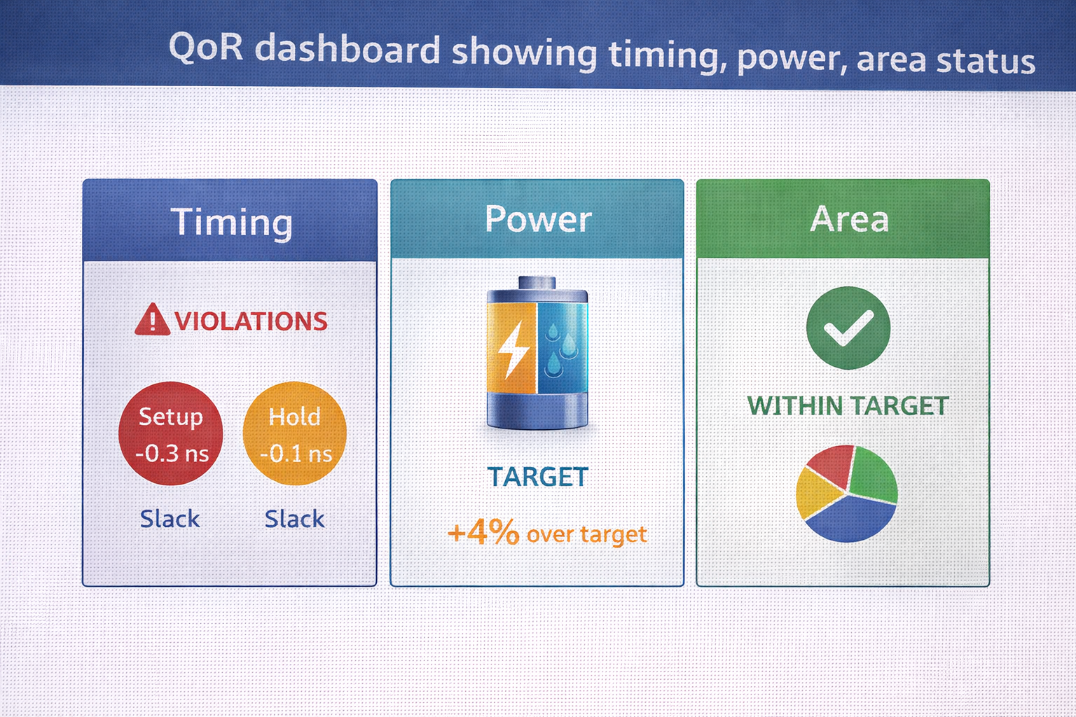
What Is QoR?
Single report summarizing Timing, Area, Power
Command
report_qor
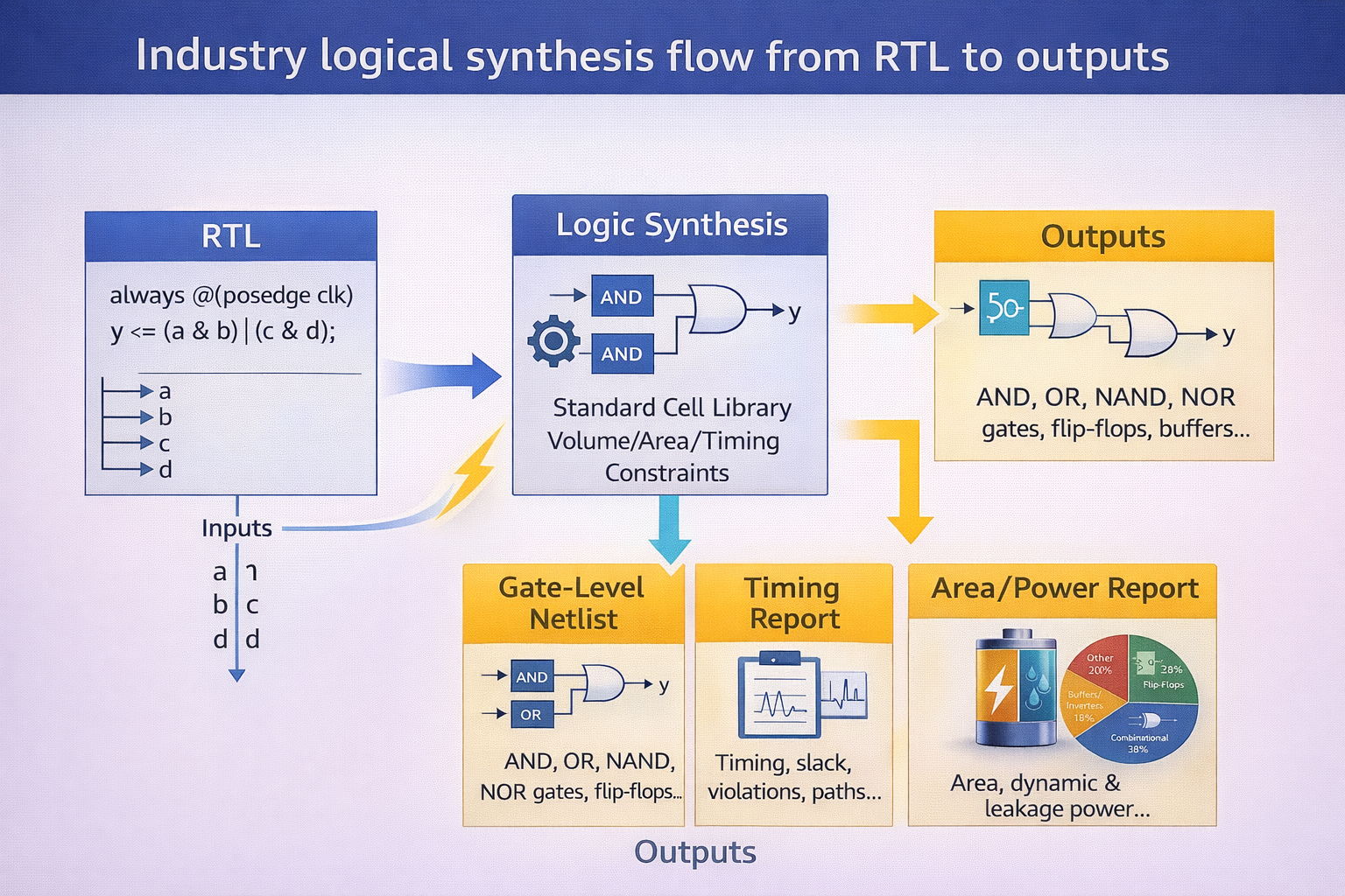
Industrial-Level Logical Synthesis Flow (Step-by-Step)
Now REAL FLOW, not theory.
Step 1. Read Libraries
set target_library "slow.lib"
set link_library "* slow.lib"
Step 2. Read RTL
analyze -format verilog {top.v block1.v block2.v}
elaborate top
Step 3. Link Design
link
Step 4. Apply Constraints
source design.sdc
Step 5. Compile
compile_ultra
Step 6. Reports
report_timing
report_area
report_power
Step 7. Write Outputs
write -format verilog -hierarchy -output top_gates.v
write_sdc top.sdc
write -format ddc -hierarchy -output top.ddc
1.1. analyze vs elaborate vs read_verilog
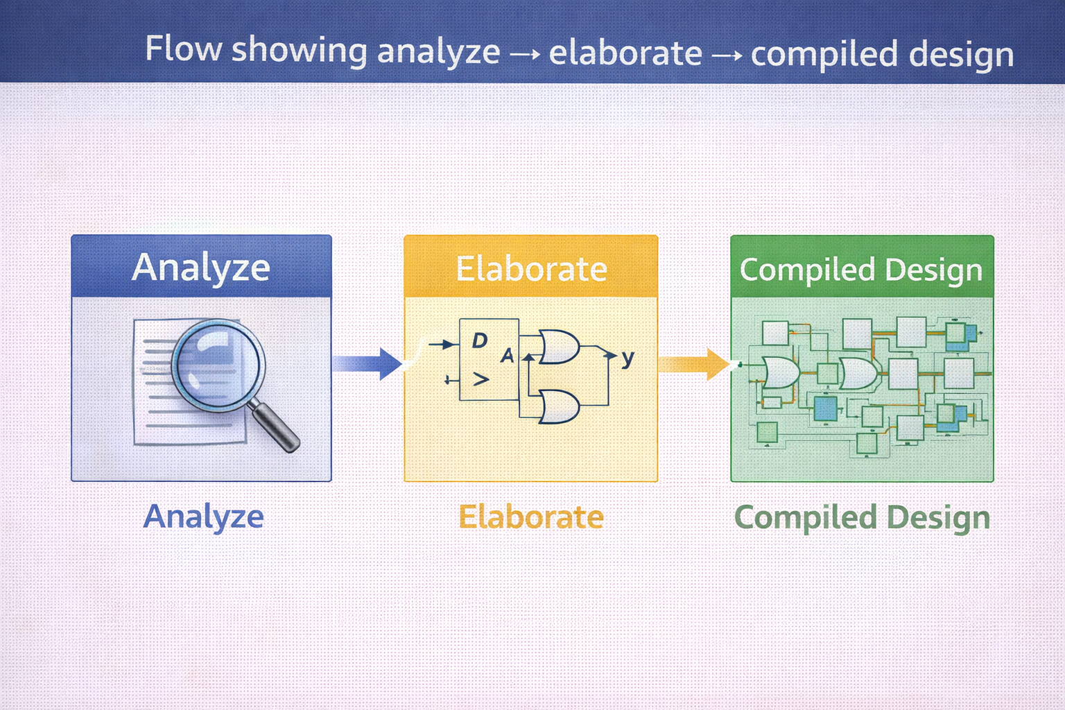
analyze
- Checks syntax
- Converts RTL to intermediate form
- No design creation
analyze -format verilog design.v
elaborate
- Builds design hierarchy
- Resolves parameters
- Creates actual design
elaborate top
read_verilog
- analyze + elaborate together
- Faster for simple designs
read_verilog design.v
Interview Difference Table
Command | Purpose |
analyze | Syntax + parse |
elaborate | Build design |
read_verilog | Both combined |
1.2. Important Topic
✔ Link stage ✔ QoR analysis ✔ Database handoff ✔ ECO friendliness ✔ MCMM readiness
(All are industry-critical)
1.3. Student Final Summary
- Logical synthesis produces multiple outputs
- Each output serves a different team
- Missing or wrong output = project failure
1.4. Conclusion
Logical synthesis is not about “compile only”. It is about clean, correct, reusable outputs.
Linking Stage (Very Important – Often Missed)
What is Linking?
After elaboration, the tool must:
- Match RTL cells → library cells
- Resolve references across hierarchy
link
Why Important?
- Prevents unresolved references
- Ensures correct library usage
Industry Interview Question What happens if link fails? ✔ Netlist cannot be generated
Image Prompt
“RTL modules linked with standard cell library blocks”
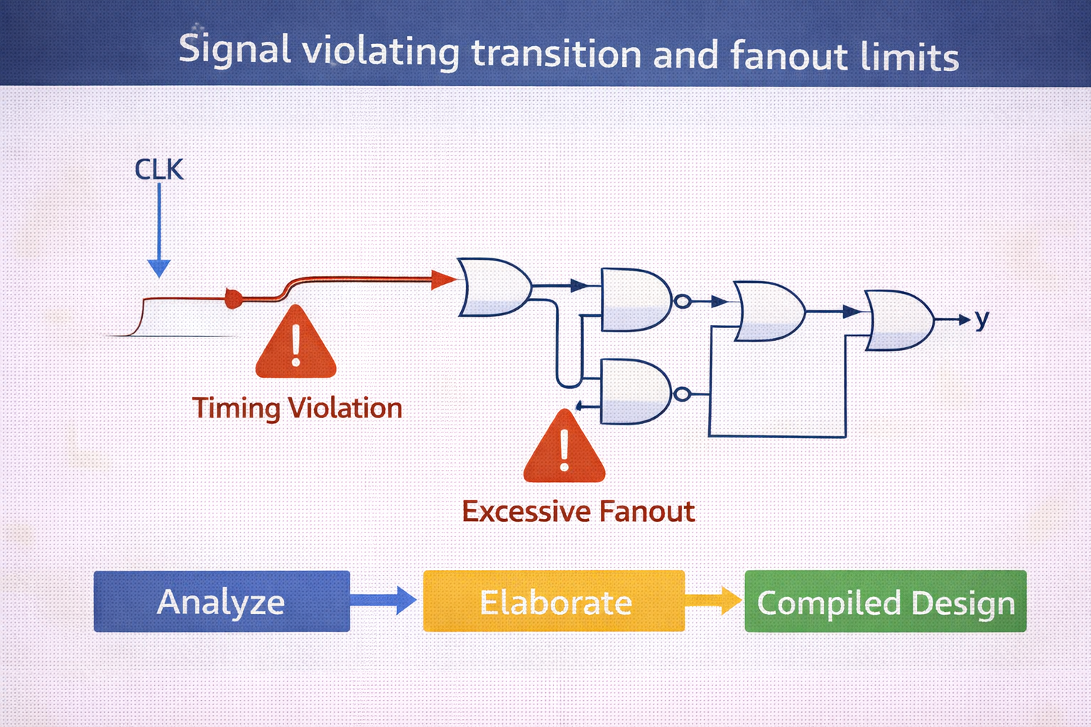
2. Design Rule Constraints (DRC at Synthesis Level)
What Are These?
- Max transition
- Max capacitance
- Max fanout
set_max_transition 0.2 [all_outputs]
set_max_fanout 8
Why Important?
- Prevents routing & timing issues later
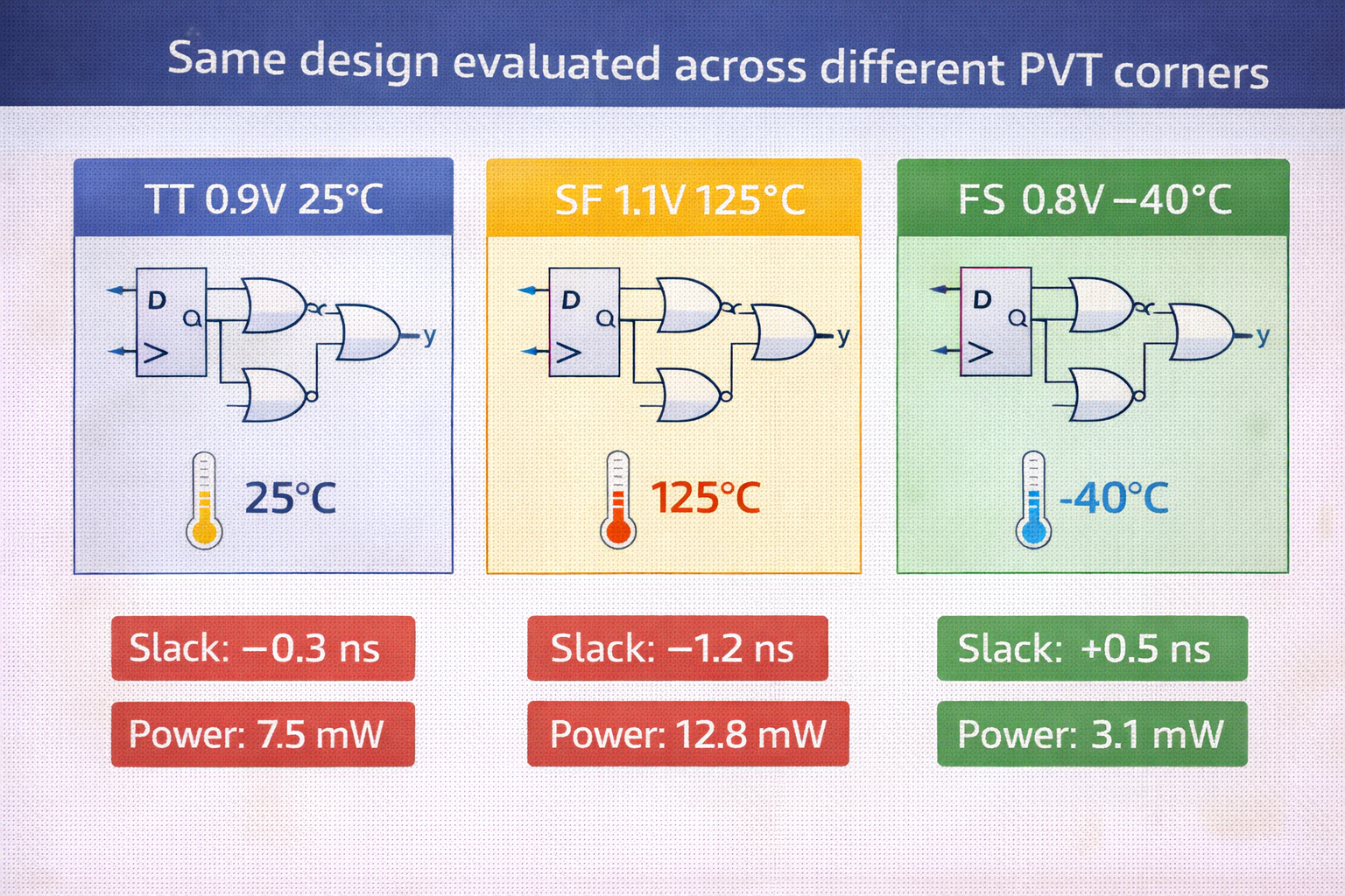
3. Multicorner Multi-Mode (MCMM) Awareness
What Is MCMM?
Design must work across:
- Multiple corners (SS, TT, FF)
- Multiple modes (functional, scan)
Even if full MCMM is done later, synthesis must be MCMM-aware.
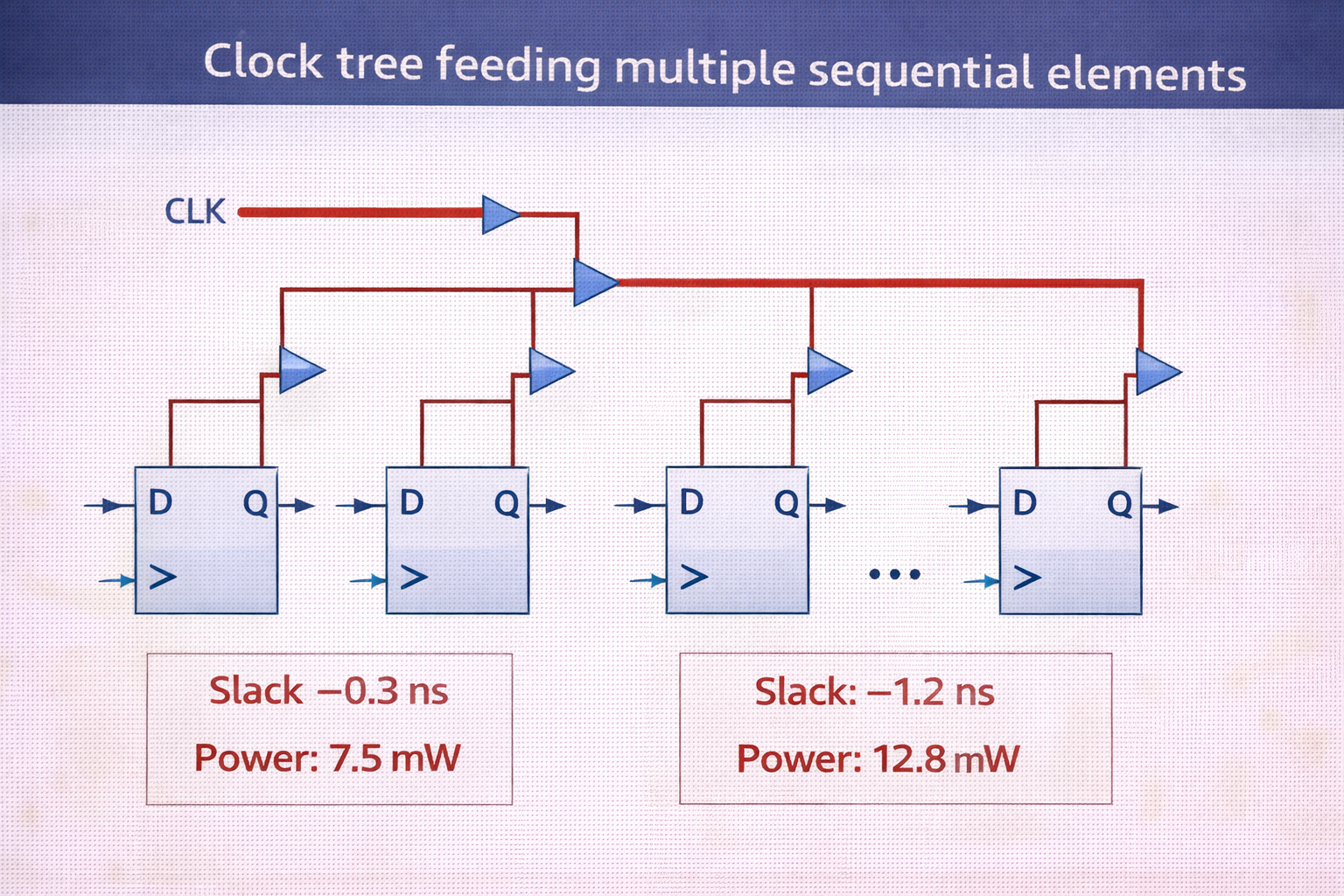
4. Clock Definition & Clock Quality
Why Clock Is Special?
- Clock drives everything
- Bad clock = bad chip
create_clock -name clk -period 10 [get_ports clk]
Tool Optimizes:
- Clock path
- Clock latency
- Clock skew (pre-CTS assumptions)
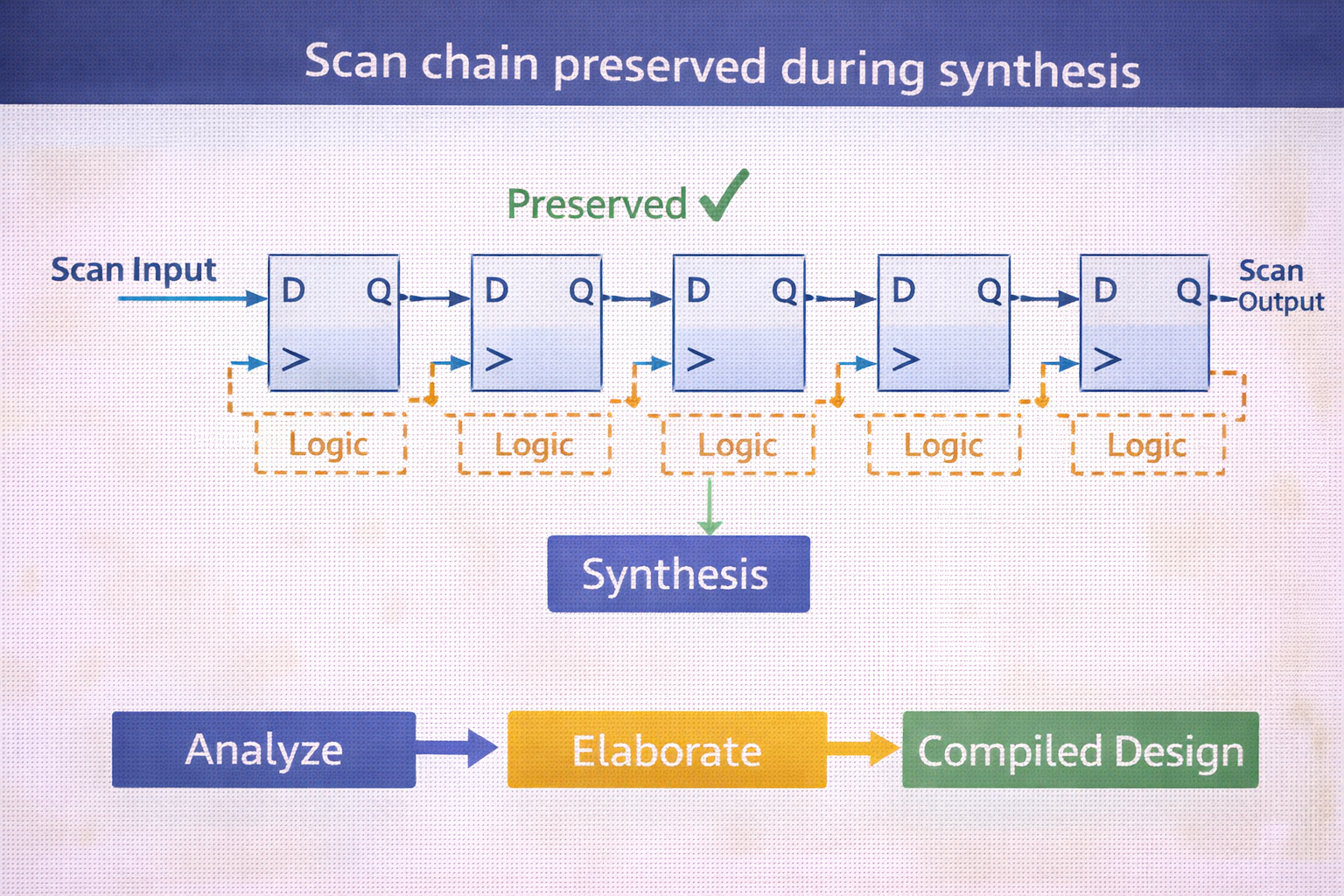
5. Scan & DFT Awareness in Synthesis
Even if DFT insertion is separate, synthesis must:
- Preserve scan ports
- Respect scan_enable
- Avoid optimizing scan logic wrongly
set_dont_touch [get_ports scan_enable]
6. Formality / LEC Readiness
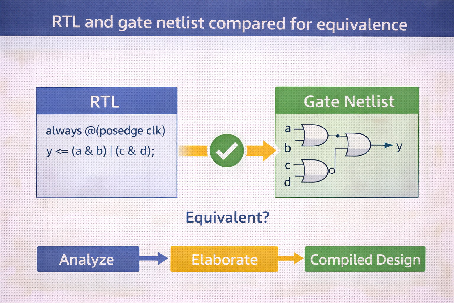
What Is LEC?
Logical Equivalence Check:
- RTL vs Gate netlist must match
Why Synthesis Must Care?
Bad optimization = LEC failure
Industry Expectation ✔ Netlist must be formally equivalent
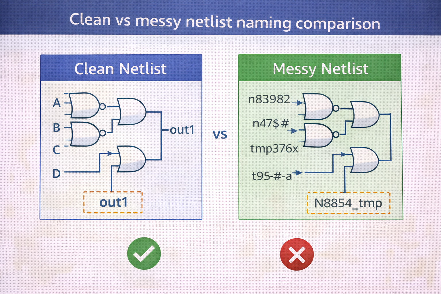
7. Naming Rules & Netlist Cleanliness
Why Naming Matters?
- PNR tools are strict
- Bad names → tool errors
set verilogout_no_tri true
set bus_naming_style {%s[%d]}
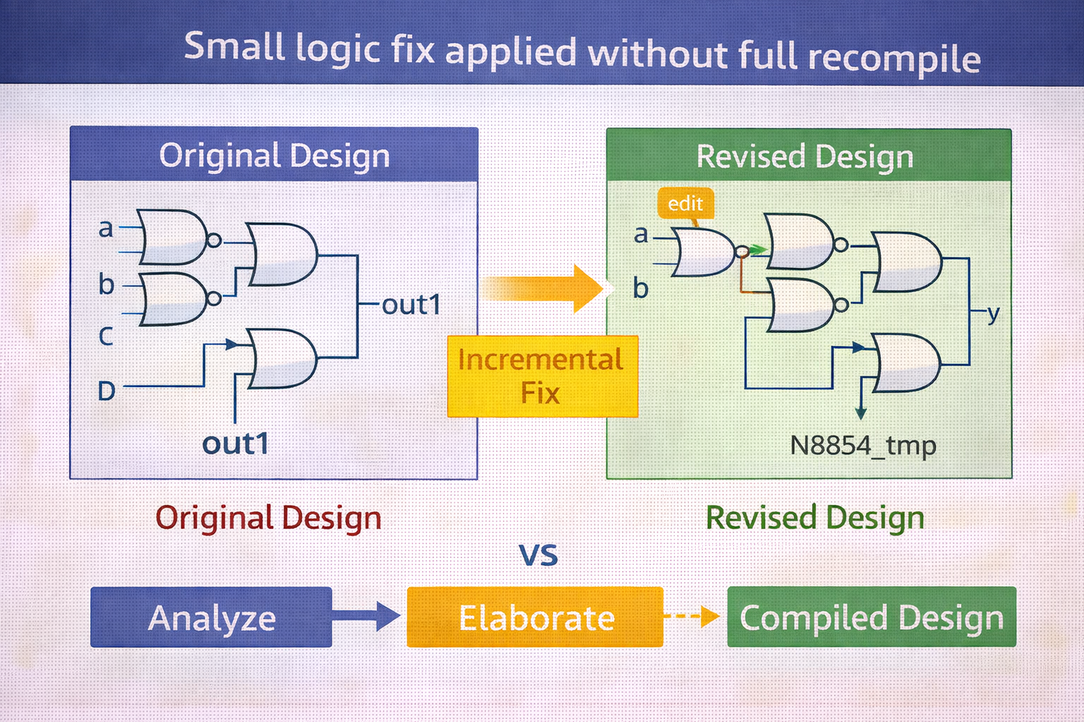
8. ECO Friendliness
What Is ECO?
Small fixes without re-synthesizing full design
How Synthesis Helps?
- Preserving hierarchy
- Saving DDC
- Avoiding aggressive flattening
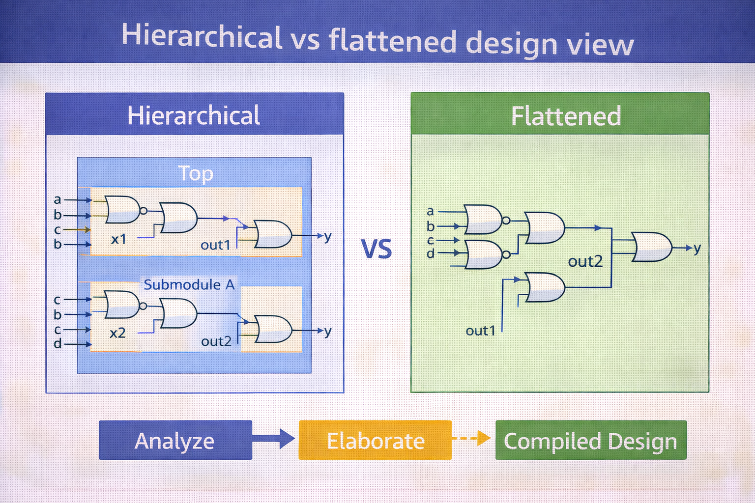
9. Hierarchy Control (Flatten vs Preserve)
set_flatten false
Why Important?
Reason | Impact |
Debug | Easy |
ECO | Faster |
PNR | Controlled |
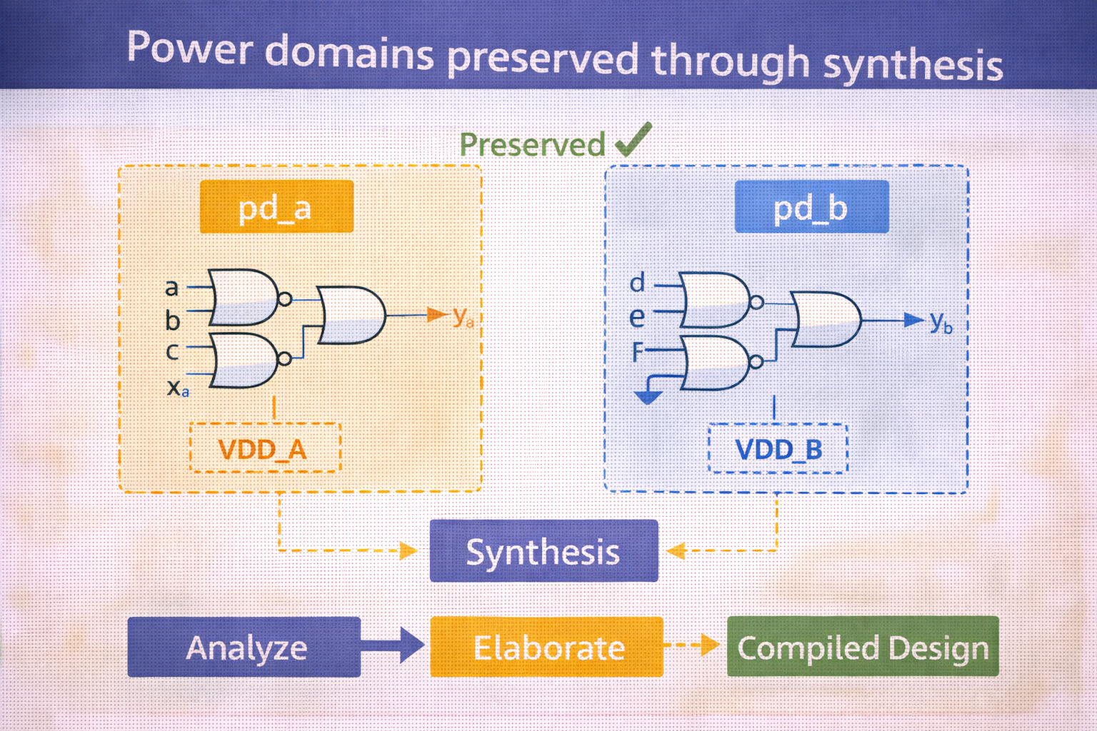
Low-Power Intent Awareness (CPF/UPF – Intro Level)
Even if power is handled later:
- Synthesis must not break power intent
- Isolation / retention logic must be preserved
STEP BY STEP PROCESS OF LOGICAL SYNTHESIS USING DC
Step1: create a directory for your new project like ORCA, ARM (mkdir ORCA, cd ORCA )
Step2: give the permission to that directory (source .cshrc file)
Step3: launch the dc_shell using below command
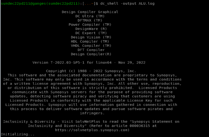

dc_shell: This is the name of the Synopsys Design Compiler command line shell, which is used
for logic synthesis.
-output: This is a command line option that specifies the name of the output file generated by
the dc_shell. In this case, the output file will be named as ALU.log you can specify any name according to your requirements
ALU.log: This is the name of the output file that will be generated by dc_shell.
✓ The file extension .log indicates that it will be a log file, which typically contains
information about the synthesis process, including any errors or warnings that were
encountered.
✓ A .log file allows designers and engineers to record this output for later review,
debugging, documentation, progress tracking, and optimization analysis.
✓ Overall, a .log file is an essential tool for designers and engineers who need to
synthesize complex designs and ensure that they are functioning correctly.
Step4: search_path
➢ The search_path command is used to specify the directories where the tool should
search for files that are included in the design.
➢ By specifying the search_path command, the user can tell the tool where to look for
files without having to specify the full directory path every time. This can save time
and effort and make the design process more efficient.
Reasons to Provide a Search Path
➢ If we don't specify a search path in your design, the tool will use its default search path
to find any files that are not in the current directory. However, if we have files in a
different directory that are not included in the default search path, the tool may not be
able to find them, which can result in errors during compilation.
➢ Therefore, it is mandatory to specify a search path to ensure that all required files are
found and compiled correctly.
➢ The figure shows the command for setting the search_path. In the search_path, we
specify the locations of the .db and. v files. because,
➢ When we instantiate a module in our design, the tool needs to know the location of
those files to be able to compile and link the design properly.
➢ By specifying the path locations of the .db and. v files in the search_path, we are
telling the tool where to look for those files during compilation.

"set" is a command that is used to modify or set a value in a software tool.
"Search_path" is a variable that specifies the directories where the software tool should look
for files and resources.
➢ if the search_path is not specified and the target_library is set directly, the tool will look
for the required files in the current working directory (CWD) and the default directories
specified in the tool settings.
➢ If the required files are not found in these locations, the tool will generate errors and
fail to compile the design.
Step5: setting link and target libraries
Reason to provide set target_library and set link_library at beginning
In the DC Shell compiler, the link and target libraries are specified at the beginning of the
compilation process for a few reasons:
➢ Library Mapping: The link and target libraries are used to map the input design to the
desired technology libraries. By specifying the link and target libraries at the beginning,
the compiler can determine the correct library mapping for the design.
➢ Optimization: The compilation uses the information from the link and target libraries
to optimize the design. By knowing the target library, the compiler can optimize the
design to meet the specified timing, power, and area constraints.
In summary, specifying the link and target libraries at the beginning of the DC Shell
compiler is necessary for accurate library mapping, optimization, and timing analysis. This
information is needed throughout the compilation process, so it makes sense to specify it
at the beginning
Target_libaray
➢ The target_library is the collection of standard cells that the program uses during the
optimization process to map the design.
➢ By specifying the target_library in our design, we are telling the compiler which set of
standard cells to use during the optimization process.
➢ The target library is used during compilation to create a technology-specific gate-level
netlist.
➢ DC optimization selects the smallest gates that meet the required timing and logic
functionality If we do not provide the target_library, the compiler program will not be
able to select the suitable components for the design, which can result in the design not
meeting its requirements or not working at all. Fig. shows the command for set
Target_library

Reasons to Provide Target Library
If you don't provide a target library, the compiler won't know which set of technology
libraries to use to implement your design.
Without a target library, the DC Shell compiler will not be able to perform library mapping,
optimization, or timing analysis accurately. It may use default libraries, which are not
optimized for your specific technology and design, resulting in suboptimal performance, power
consumption, and area usage.
In the command "set target_library", each word refers to the following:
"set": This is a command used to set a variable.
"target_library": This is the name of the variable or option being set in the program. It refers
to the collection of standard cells that the program will use during the optimization process to
map the design.
link_library
➢ The link_library variable is used to specify a list of libraries and design files that can
use to resolve references when a design is loaded.
➢ The link command links all the referenced components and designs to the current design
to make it complete.
➢ An asterisk (*) in the link_library variable specifies that Design Compiler should search
memory for the reference.
➢ The "*" symbol in the link_library command is used as a wildcard character to include
all the libraries in the current directory that match a specific pattern.
➢ Using the "*" symbol in the link_library command makes it easier and faster, to include
all related libraries without manually listing them one by one. It saves time and effort
and reduces the chances of errors while specifying the command.
To “resolve” the reference DC (A ‘reference’ is any gate, block, or sub-design that is
instantiated in our design):
✓ First looks in DC memory for a matching design name.
✓ Next look in the technology libraries listed in the link_library variable for a matching
library cell name.
The figure shows the command for setting the link_library path.

In the command set link _library, each word refers to the following,
➢ "set" is a command to set a particular value to a specified variable or parameter
➢ "Link_library" refers to the variable that stores the list of libraries and design files
that the Design Compiler can use to resolve references.
➢ If Design Compiler does not find the reference in the link libraries, it searches in the
directories specified by the search_path variable.
➢ If we don't specify the link_library correctly, the tool won't find the necessary files and
libraries for the design, resulting in errors during the design process.
➢ The temporary files generated by the analyze command will also be affected, making it
difficult to create a fully functional design. So, it is important to provide a link library
during the synthesis process.
Below Fig. explains how the warning will come, if link_library is not provided properly or if
link_library is not given in our design.
Step6:Reading files
There are two methods to read the files into Dc.
✓ analyze and elaborate
✓ read_file command.
Read Verilog
✓ The read_file command analyzes the design and translates it into a technology-
independent (GTECH) design in a single step.
✓ read_verilog includes two steps, that is, analyze and elaborate, but do not link the
design automatically.
Reading verilog files using analyze command
Through analyze and elaborate command you would specify the directory where you want
the design files to be stored but in the case of read_file, the design files would get
automatically stored in the present working directory.
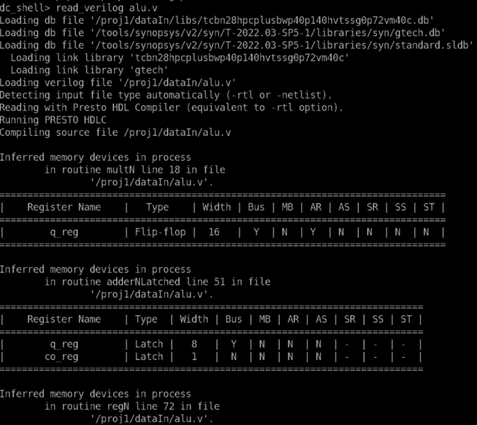
Read_file
Reads designs and libraries into memory
➢ Performs the same operation as analyzing and elaborating in one step.
➢ Does not create intermediate files for Verilog
➢ Creates intermediate files for VHDL
Does not execute the link command automatically. The link has to be done manually
after the read_file command.
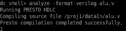
Analyze
The "analyze" command reads source code files written in Verilog or VHDL hardware
description language (HDL), checks for syntax errors and issues warnings or errors, reports
errors, and converts the source files into machine code. When the files are converted, the
resulting binary files are placed in the current working directory (CWD).
The "-format verilog" option specifies that the source files are written in the Verilog language.
Below Fig. shows the command for Analyze, in our design, we are using the Verilog files which
is why we are considering the option -format Verilog.
Finding the Top – Module name in our design
➢ To find the top module name in a Verilog design,
➢ Open the Verilog design file in a text editor, with the help of the command. The below
command helps to open the Verilog file.

➢ Sh, gvim is a command used to start a graphical text editor called gvim.
➢ gvim is a text editor that runs in a graphical environment.
➢ To open the Verilog file the command sh gvim was executed
➢ Look for the module definition at the beginning of the file. The module definition starts
with the keyword module, followed by the name of the module and a list of input and
output ports.
➢ Top module name will be one it should not call in any other module
Elaborate
The "elaborate" command combines various modules and components of a circuit described in
a file (in Verilog or VHDL format) to create a complete circuit design for simulation testing.
The steps that happen in Elaborate Command are:
➢ At this stage, it reads the RTL code, and this RTL code is converted into modules as per
its logical hierarchy.
➢ Once it has all logical Boolean representation loaded, the tool maps logic with a
technology-independent cell called the Gtech cell.
➢ During elaboration, the tool checks whether the design is unique, if not, it stops the
tool. Once the design becomes unique, the tool checks for unresolved references in
the design.
➢ If it has linking issues, then an RTL correction is required, or you need to check if
it is due to any missing libraries.
➢ After elaboration, it checks for timing loops in design. If you find any timing loop,
you need to get the RTL correction done by the designer.
➢ The top module is the main thing in a design, containing lower-level modules. When
using the elaborate command to create a netlist, we must provide the top module
name as input.
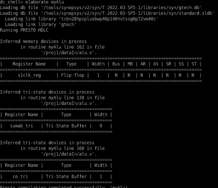
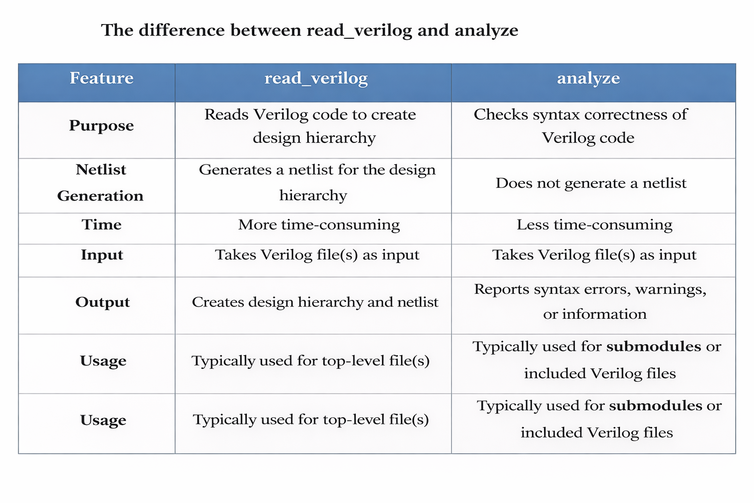
Compile
Compile command performs both logic level and Gate – level netlist synthesis and optimization
on the current design.
The compile command performs the following steps:
➢ Perform optimizations such as technology mapping, and cell replacement to generate a
netlist that is optimized for the target technology.
➢ Generate a report that lists any errors or warnings detected during the process.
➢ Convert the netlist into the target technology format such as Gtech format, which is
used by Synopsys tools for implementation and verification.
➢ After elaboration, in the compilation stage, the tool maps the Gtech cell with the actual
cell (specific technology dependent) from the library. Actual cell mapping is dependent
on design constraints or user-specific constraints. Apart from this, the tool removes the
registers with constant propagation/unloaded which are not required in the design. If
these removed cells are required, then you need to provide feedback to the designer to
get the correct RTL.
➢ After elaboration and compilation, the tool performs optimizations based on user
constraints to meet timing, area, and power requirements.
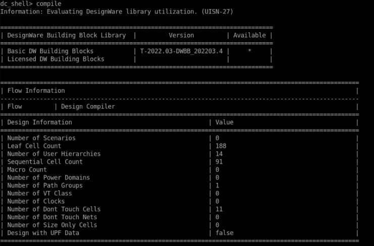
Once the compilation process is complete, the netlist is ready for various design activities such as Schematic view, Apply SDC,static timing analysis, and power analysis etc.
Start_gui
➢ The start_gui command is used to open the graphical user interface (GUI) of the tool.
➢ This allows the user to visually interact with the tool Below Command opens the
schematic view of design

Stop_gui
➢ The stop_gui command is used to close the graphical user interface (GUI) of the tool.

NOTE : After the elaborate command, the compile command is to optimize the netlist for the target
technology.
The compilation process includes technology mapping, and cell replacement, along with
verifying the netlist for timing and logical errors.
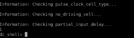
Check_timing
✓ The "check_timing" command is to identify any possible timing problems in a design.
✓ To check for constraint problems such as undefined clocking, undefined input arrival
times, and undefined output constraints, we use the check_timing command.
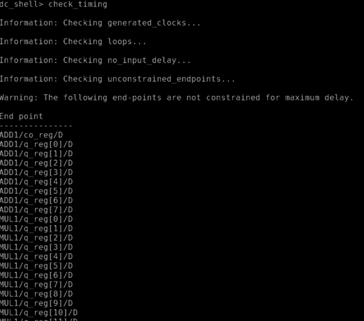
all_inputs
➢ The "all_inputs" command is used to gather a list of all input or inout ports in the current
design.
➢ It returns a collection of these ports and can be useful for analyzing and controlling
input data in a design.
Below is the command for all_inputs. When this command is executed, it returns a list of all
the input or inout ports that exist in our design.

all_outputs
➢ The all_outputs command is used to get a list of all output or inout ports in the current
design.
➢ It can be used to search for specific output ports, on all output ports at once.
Below is the command for all_outputs. When this command is executed, it returns a list of all
the output or inout ports that exist in our design.

all_registers
➢ The all_registers command is used to get a list of all the pins in the current design. By
default, it will return a list of all the pins in the design.
Below is the command for all_registers When this command is executed, it returns a list of all
registers that exist in our design.

all_registers -clock_pins
➢ The command all_registers -clock_pins is used to find and return a list of clock pins in
the current design.
Below Fig. shows the all_registers -clock_pins command returns a list of clock pins in the
current design.

Size_of Collection
The sizeof_collection is a command, used for determining the number of objects in the
Collection.
With the help of the below command, we can know how many clock pins are there in our
design.

all_fanin
➢ The all_fanin command in synthesis is used to identify all the input signals of a
particular signal or a group of signals.
all_fanin -to
The "all_fanin -to" command is used to find all the input sources connected to a particular
output in a design, making it a useful tool for identifying inputs to a specific gate or register.
The below command executes every register of the clock pin, as the ALU design consists of 76
clock pins. For example, let us consider one clock pin in our design,

all_fanin -to -flat : command help to get a list of all the clock pins
associated with registers in the current design, while also flattening the design structure.

The "all_fanin -to -flat -startpoints_only" command can be used to identify the
start points associated with clock pins in a flattened design structure. The start points are the
pins or nets where the paths start.

let us consider another clock pin in our design,

We can clearly observe that while giving -flat switch in this clock pin, ‘MUL1/q_reg[0]/CP’we
can see that the clock pin consists of flat cells.

The below command shows the starting points for the clock pin of MUL1/q_reg[0]/CP

So, design because of more number of clock pins, manually it takes more time to see
the start points of every clock pin. With the help of the above commands, we can write a script
to find the number of clocks in our design in dc_shell in genus we have direct command [get_clock_ports ].
# Loop through all registers clock pins
foreach i [get_object_name [all_registers -clock_pins]] {
# Get all fan-in start points
set a [get_object_name [all_fanin -to $i -flat -startpoints_only]]
# Check if list is not empty
if {[llength $a] == 1} {
# Loop through all primary inputs
foreach j [get_object_name [all_inputs]] {
# Compare fan-in with input
if {$i == $a} {
lappend c $a
}
}
}
}
# Print unique sorted list
puts [lsort -u $c]

We need to source the above file in shell will get the clock ports name need to create the clock for those ports
Create_clock
➢ The "create_clock" command creates a clock in a design by defining its source, which
can be pins or ports.
➢ Only one clock can be associated with a pin or port. If no sources are specified, a virtual
clock can be created using the clock name.
In the below command, the command creates a clock with the name "CLK" and a period of 10
nanoseconds.
The "-name" option specifies the name of the clock, while the "-period" option sets the clock
period to 10 nanoseconds.
The "[get_ports clk]" option selects the port named "clk" as the source for the clock. This means
that the "clk" port is defined as the source for the clock signal with a period of 2 nanoseconds.

In the below command, the command creates a clock with the name "CLK" and a period of 5
nanoseconds.
The "-name" option specifies the name of the clock, while the "-period" option sets the clock
period to 5 nanoseconds.
The "[get_ports clk]" option selects the port named "clk" as the source for the clock. This means
that the "clk" port is defined as the source for the clock signal with a period of 5 nanoseconds.

Report_clocks
The “report_clock” command displays important information about the clock network in a
design. It shows the details like clock groups, clock period, clock latency, and other clock
constraints. To use it, enter the command in the interface.
The below command shows the clock report for “CLK and I1”
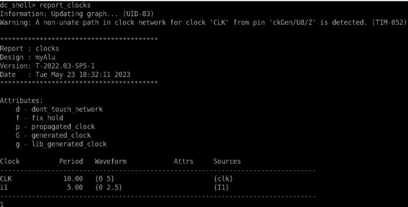

Need to execute again check timing command to know the other violations warning errors
Check_timing
The "check_timing" command is to identify any possible timing problems in a design.
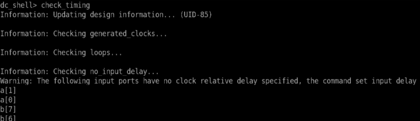
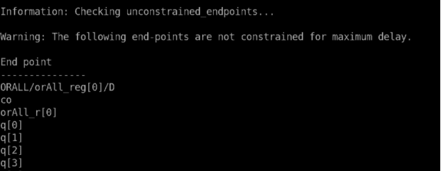
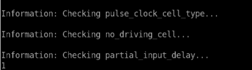
Set_input_delay
➢ The "set_input_delay" command allows setting the delay time for a signal to travel
from an input pin to a register in a design.
➢ It helps that the input signal arrives at the right time and is properly captured by the
register.
Below Fig. The "set_input_delay" command is used to set input path delay values in a design.
In this, a delay value of 6 nanoseconds is being set for all input signals except for those
connected to the "clk" clock. The "remove_from_collection" command is being used to remove
the clock and apply it to all input signals connected to the "clk" clock.
If we don't know the exact time for the signal to arrive at the input port or output port, we will
keep a pessimistic value of 60 % to the external world and 40 % to our design.
And the input delay is not a constant value. Worst case, we will assume 60% and company to
company changes the input and output values.

Like this you need to apply input delay for all the output ports with respect to other clock NOTE: when we are define input delay for other clock need to add -add option to command not to override previous command
➢ -add_delay We use this switch because the previous input delay of the clock should not
replace with another clock of the output delay.

Set_output_delay
➢ The set_output_delay command is used to set the time delay between a clock edge and the
output signal on output ports in a design.
➢ It's important to specify the delay and meet timing requirements.
➢ In this case, the delay being set is 6 nanoseconds of time, and it is applied to all output
ports in the design using the "all_outputs" command.

After apply input delay output delay respected to all the clocks we need to do again check_timing command for to find remaining warnings and errors
Check_timing
➢ The "check_timing" command is to identify any possible timing problems in a design.
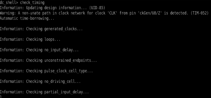
The above fig shows after clearing all the input delays and endpoints it is showing the non –
unate path in the design. To know the command for the non-unate path, we can man the error
code which was shown in the check timing i.e., TIM -052
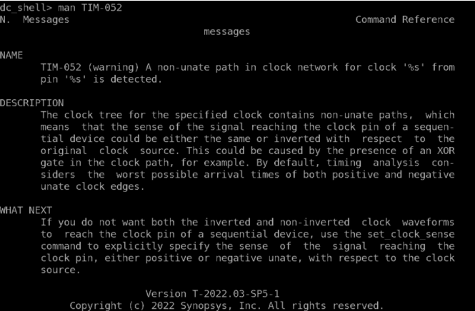
By doing the man for that error code we can see in the above fig it shows the line ‘what next’
by reading that description we can find out which command can be used to remove the non-
unate path in our design.
Timing sense of an arc: The timing sense of an arc is defined as the sense of traversal from
the source pin of the timing arc to the sink pin of the timing arc. Timing sense is also called as
"unateness" of the timing arc.
Non-Unateness
The non-unate represents a function where a change in output value cannot be determined from
the direction of the change in the input value. The output pin value is not dependent on the
single input pin. It also depends on 2nd input pin. Since the timing arc will be between the single
input and single output pin, so, it’s difficult to identify this relationship directly.
The below figure shows the block diagram of the clock generator, this is the block that contains
the non-unateness path in design.
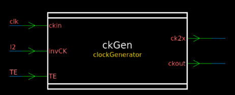
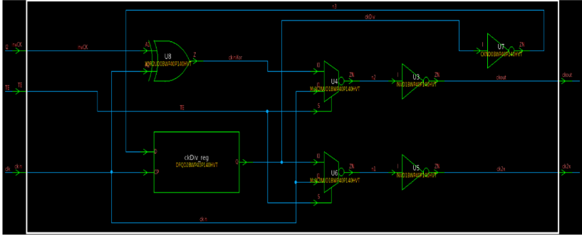
In the above figure, we can see the xor gate with two input pins, i.e., I2 and clk. So, for this
gate, the non-unateness is happening. The output pin value is not dependent on the single input
pin. It also depends on 2nd input pin. So, we can’t change the clk and the other input for the xor
gate is the I2 pin, for this we need to set 0 (constant) for the I2 pin.
So, with the help of set case analysis, we can set the value.
Set case analysis
Specifies that a port or pin is at a constant logic value of 1 or 0.
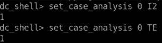
The above fig shows that we are making a constant logic value ‘zero’ for the I2 pin, we are
setting ‘zero’ for the TE pin also because the output of the xor gate is the input for the Mux,
for that Mux the TE is the selection pin so the selection line allows the multiplexer circuit to
switch its “attention” between the various input data lines when determining the value to be
output. That’s why we are setting zero for the TE pin.
Difference between set clock sense and set case analysis
Set clock sense
This command only is meaningful in the context of a non-unate clock network. To specify the
unateness of the clock network, the user needs to specify the name of the design pins through
which the clock passes.
Set case analysis
Case analysis is a way to specify a given mode of the design without altering the netlist
structure. For the current timing analysis session, you can specify either that some signals are
at a constant value (1 or 0) or that only one type of transition (rising or falling) is to be
examined. When you specify case analysis to a constant value, the constant value is propagated
through the network as long as a controlling value for the traversed logic is at the constant
value.
Report_transitive_fanin
Reports logic in the transitive fanin of specified sinks.
In check timing, we can observe that unconstrained endpoints are removed but there is a
warning message i.e., a non-unate path is there for the pin ckGen/U8/z. so, to know the sense
of this we can use the command report_transitive_fanin
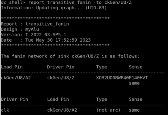
Check_timing
➢ The "check_timing" command is to identify any possible timing problems in a design.
The below check timing shows that the non-unate has been removed.so, after clearing the non-
unate path, it’s showing that some of the endpoints are not constrained for the maximum delay
for that we need to apply the output delay with respect to clock.
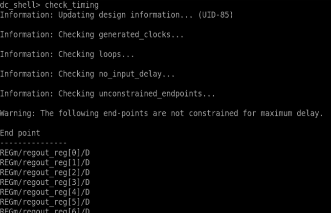
Generated clock
A generated clock is one that is derived from another clock, known as its master clock by a
circuit within the design itself, such as a clock divider. These are divider/multiplier clocks that
get generated from a master clock. The generated clock may be of the same frequency or a
different frequency than its master clock.
Mostly these are defined at the output of a clock divider like a flip-flop or mux. When we define
a generated clock, its source clock, the generation point, and division ratio should be provided.
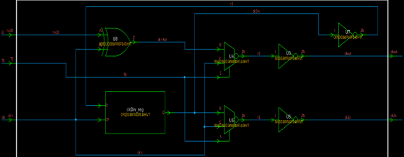
The above fig shows that the ckDiv_reg block is the divider by circuit. So, that’s why we create
the generated clock in our design.
The below figure shows the command to create the generated clock in Alu design.

The "create_generated_clock" command is used to define a clock name "gen" in the design.
The source clock for this clock is "clk". The frequency of the generated clock is half of the
source clock, and it is associated with the Q pin of the "ckDiv_reg" register within the "ckGen"
module.
Report_clocks
The “report_clock” command displays important information about the clock network in a
design. It shows the details like clock groups, clock period, clock latency, and other clock
constraints. To use it, enter the command in the interface.
The below command shows the clock report for clk, I1, gen.
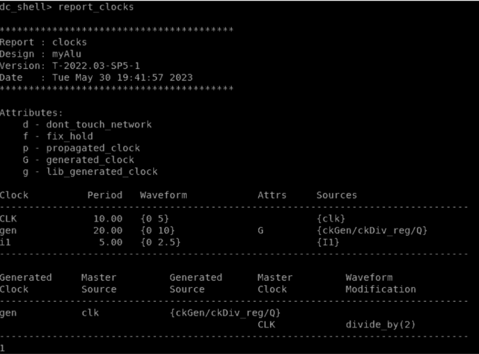
Check_timing
➢ The "check_timing" command is to identify any possible timing problems in a design.
The below fig shows that check timing is clear after creating the generated clock.
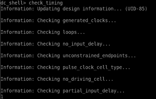
Clock uncertainty
➢ Clock uncertainty is the deviation of the actual arrival time of the clock edge with
respect to the ideal arrival time. In ideal mode, the clock signal can arrive at all clock
pins simultaneously.
➢ But in fact, that perfection is not achievable. So, to anticipate the fact that the clock will
arrive at different times at different clock pins the ‘ideal mode’ clock assumes a clock
uncertainty.
➢ To define a clock uncertainty, we have to use the command set_clock_uncertainty.
Set clock uncertainty
This command checks if the clock signal timing is uniform throughout the design, which is
important for the circuit to work correctly.
Uncertainty has the following factors:
Jitter: Jitter is a deviation of the clock signal from its ideal timing
Margin: Margin is the safety buffer in a system for reliable operation under varying conditions.
Crosstalk: Crosstalk is the coupling of signals between adjacent wires or components in a
digital circuit.
Skew: Skew is the difference in arrival times of the clock signal at different parts of a circuit.
We take 20 % uncertainty for setup (jitter+Margin+crosstalk+skew) and 15 % uncertainty for
hold (Margin+crosstalk+skew)

The above fig represents, how uncertainty is applied to CLK
Command: set_clock_uncertainty -setup 2 [get_clocks CLK]
Explanation:
✓ set_clock_uncertainty: Specifies the command to set clock uncertainty for timing
analysis.
✓ -setup: Indicates that the clock uncertainty being set is for setup timing.
✓ Sets the setup clock uncertainty value to 2 units.
✓ [get_clocks CLK]: Retrieves the clock signal named "CLK" from the design.
Command: set_clock_uncertainty -hold 1.5 [get_clocks CLK]
Explanation:
✓ -hold: Indicates that the clock uncertainty being set is for hold timing.
✓ Sets the hold clock uncertainty value to 1.5 units.

The above fig represents, how uncertainty is applied to the i1 clock
Command: set_clock_uncertainty -setup 1 [get_clocks i1]
Explanation:
✓ set_clock_uncertainty: Specifies the command to set clock uncertainty for timing
analysis.
✓ -setup: Indicates that the clock uncertainty being set is for setup timing.
✓ Sets the setup clock uncertainty value to 1 unit.
✓ [get_clocks CLK]: Retrieves the clock signal named "i1" from the design.
Command: set_clock_uncertainty -hold 0.75 [get_clocks i1]
Explanation:
✓ -hold: Indicates that the clock uncertainty being set is for hold timing.
✓ Sets the hold clock uncertainty value to 0.75 units.
Driving cell
We use the set_driving_cell command to specify the drive characteristics of input or inout ports
that are driven by the cells in the technology library. These commands associate a library pin
with input ports so that delay calculation can be accurately modeled.
The syntax of the set_driving_cell command:
Set_driving_cell [-lib_cell_name]

The above fig shows after executing the Set_driving _cell command it is showing some
warning message in the design. So, there we can man the error code i.e., UID -401.
By doing the man for that error code we can see in the above fig it shows the line ‘what next’
by reading that description we can find out which command can be used to remove the warning.
This is optional but, if we don’t want to see the warnings or errors and to know the next step
this is the way to approach and find out.
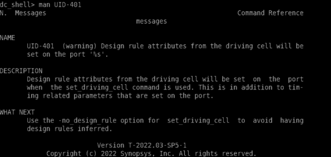
So, after doing the man to that error code, it shows the option no_design_rule to remove the
warnings. The below fig shows the warnings are removed.

Set_load
This constraint defines the capacitive load to the output port or any specified net.
set_driving_cell and set_load are commands to make sure that the interface to your P&R
block will not cause transition or capacitance violations when connected to external circuitry
in a chip.

Group_path
The grouping of paths can be done using the group_path command. It groups a set of paths or
endpoints for timing analysis and cost function calculations. Paths within a group are analyzed
and optimized separately from other groups. By default, there is one path group per clock. All
timing paths clocked by a given clock at the path endpoint belong to that clock's path group.
All timing paths within a path group are optimized for timing together, starting with the critical
path, which is the path having the worst slack within the group. After the critical path is fixed,
the next-worst path becomes the new critical path and the target for fixing. The tool continues
fixing paths until all paths in a group have zero slack or until a better optimization solution for
the current critical path cannot be found. In this case, the subcritical paths are not fixed are and
left with timing violations. Paths within a group are optimized and reported separately from
the other groups.
Group paths are automatically created when the create_clock and group_path command is used.
The default group path contains all paths not captured by a clock. We can use the report_timing
command to see which groups we have.
The below figure shows the command for creating different group paths for an Alu design.
group_path -name r2r -from [all_registers -clock_pins] -to [all_registers data_pins], the group
is named r2r, and the paths start from the clock pins of all registers (clock_pins option) and end
at the data pins of all registers (-data_pins option), like that we can create a group path for
iin2reg, reg2out, and in2out.

Report_timing
The "report_timing" command generates a detailed report with timing information for the
current design.
And also creates the group paths reports that we created. The below figure shows the report
timing all for groups that are created.
The below figure shows the report timing for clock path CLK
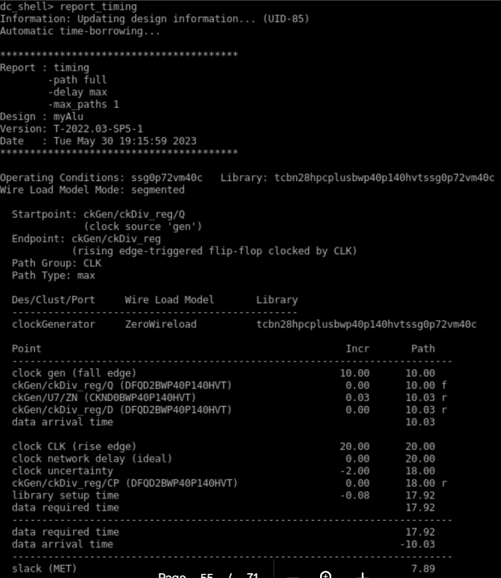
IN2OUT Port
The clock for the in2out port is outside the block and we don’t know which clock is driving
in2out.
So, we have to filter the inputs and outputs ports for the in2out path and give the delay for those
ports with respect to the clock which we created i.e., virtual clock.
To filter the input ports, below is the command to get input ports

To filter the output ports, below is the command to get output ports

VIRTUAL CLOCK
- A virtual clock can be defined as a clock without any source in other words a virtual clock is
a clock that has been defined but has not been associated with any pin/port.
- It does not physically exist in the design but it does exist in the memory. It is used as a
reference to constrain the interface pins by relating the arrivals at input/output ports.
We can simply define the virtual clock by the create_clock command but we don’t need to give
any generation point since for the virtual clock there is no actual clock source in the design,

Report clocks
The “report_clock” command displays important information about the clock network in a
design. It shows the details like clock groups, clock period, clock latency, and other clock
constraints. To use it, enter the command in the interface. To know whether the clock is
created we can use the report clocks command.
The below command shows the clock Virtual is created.
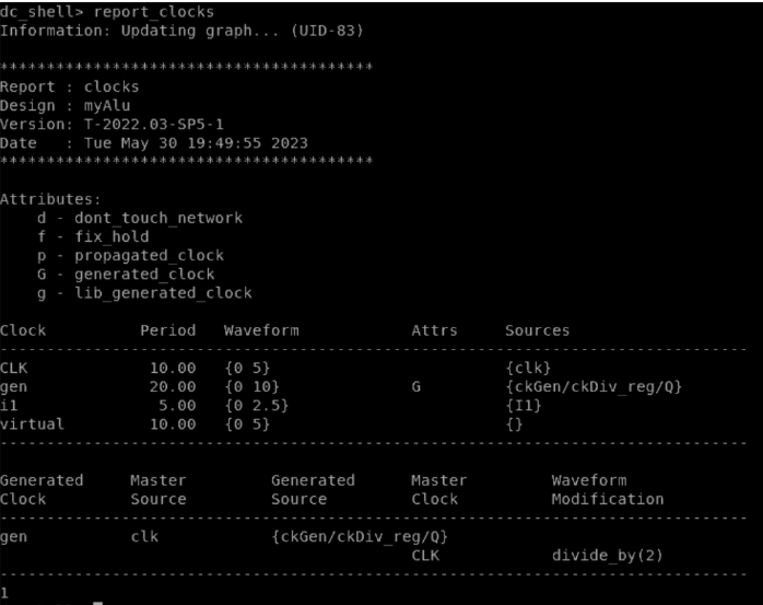
Input Delay
We give a 35% delay with respect to the virtual clock for input ports of the in2out path by
filtering those ports from the design. If we consider a 60% delay of input and output delay, no
positive percentage of timing is left to do analysis.

Similarly for output delay also we have applied 35% of the delay with respect to the virtual
clock.

NOTE: AFTER ALL THE CONSTRAIN NEED TO RUN COMPILE COMMAND ONE MORE TIME
The below figure shows, after giving the virtual clock for the in2out path the slack is met.
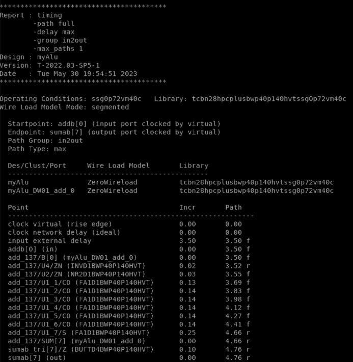
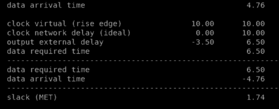
Report_qor: Displays QoR (quality of results) information and statistics for the current
Design.
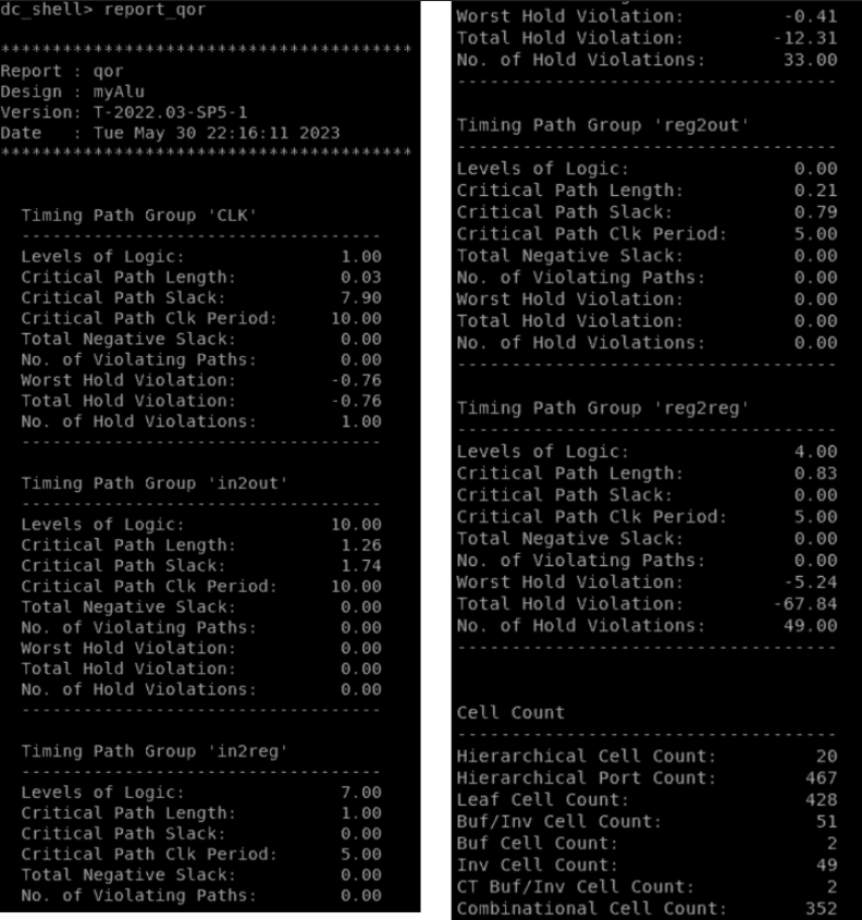
Report_area: Displays area information for the current design.
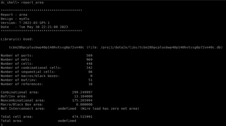
Report_power: Calculates and reports dynamic and static power for the design .
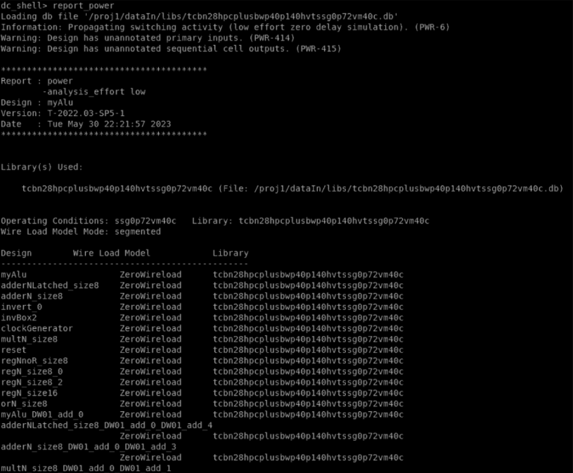
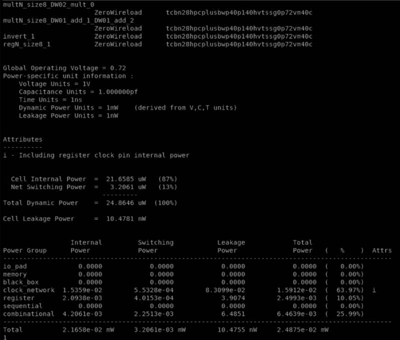
Write_file: Writes a design netlist from memory to a file.
To open this, write file we use below command in dc_shell.

Write_sdc
It generates SDC file for our current design

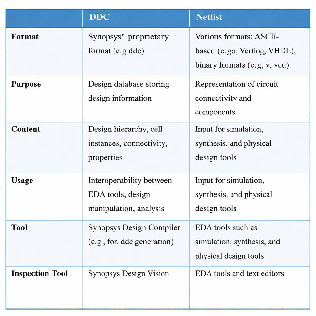
STEP BY STEP PROCESS OF LOGICAL SYNTHESIS USING Genus
1. Set the library search path (Where Genus will look for technology libraries)
set_db init_lib_search_path {./libs/}
This tells Genus where the standard cell library files are stored.
2. Set the SDC (timing constraints) search path
set_db script_search_path {./constraints/}
This tells Genus where your timing constraint file (SDC) is located.
3. Set the Verilog (RTL) search path
set_db init_hdl_search_path {./rtl/}
This tells Genus where your design (Verilog files) are stored.
4. Set the library file (technology file used for synthesis)
set_db library {./libs/tech_library.lib}
This selects which standard cell library Genus should use.
5. Read the Verilog design
read_hdl ./rtl/alu.v
Loads your RTL design into Genus.
6. Elaborate the design (build internal model)
elaborate
Genus builds the complete logic hierarchy of your design.
7. Find clock ports automatically
get_clock_ports
Genus identifies all clock signals in the design.
8. Check initial timing status
check_timing_intent
Checks if basic timing information is missing.
9. Source (load) the SDC constraints file
source ./constraints/sdcfile.tcl
This file contains all timing constraints like clock, input delay, output delay, etc.
10. (Inside sdcfile.tcl) – Clock and timing constraints
create_clock -period 10 [get_ports clk]
create_clock -period 5 [get_ports ll]
set_input_delay 6 -clock clk [get_ports [remove_from_collection [all_inputs] {ll clk}]]
set_output_delay 6 -clock clk [get_ports [all_outputs]]
set_input_delay 3 -add_delay -clock ll [get_ports [remove_from_collection [all_inputs] {clk ll}]]
set_output_delay 3 -add_delay -clock ll [get_ports [all_outputs]]
set_driving_cell -lib_cell BUFDF8BPW40P140HVT [get_ports [remove_from_collection [all_inputs] {clk ll}]]
set_load 0.00146193 [get_ports [all_outputs]]
set_clock_uncertainty -setup 2 [get_clock clk]
set_clock_uncertainty -hold 2 [get_clock clk]
set_clock_uncertainty -setup 1 [get_clock clk]
set_clock_uncertainty -hold 1 [get_clock clk]
set_case_analysis 0 TE
set_case_analysis 1 T2
create_generated_clock -name gen_clk -divide_by 2 -source clk [get_pins ckGen/ckDiv_reg/Q]
(These define clocks, input/output delays, uncertainty, loads, and generated clocks.)
11. Terminal commands (extra checks)
check_timing_intent
filter_collection [all_fanin -to [all_outputs]] "port_direction == in"
filter_collection [all_fanout -from [all_inputs]] "port_direction == out"
create_clock -name ver -period 10
set_input_delay -clock ver 3.5 [get_ports {addc.*to$}]* [TRI]
set_output_delay -clock ver 3.5 [get_ports sumab[*]]
set_false_path -from ll -to ver
set_false_path -from ver -to ll
12. After report timing fixes (multi-cycle paths)
(Kept same commands, but they are fixing long paths for timing)
set_multicycle_path -from ci -to ADD1_q_reg[7]/D -setup 2
set_multicycle_path -from ci -to ADD1_q_reg[7]/D -hold 1
..
(set of similar commands for other registers)
(These tell Genus that some paths have more than one clock cycle.)
13. Run synthesis (Translate → Map → Optimize)
syn_generic
syn_map
syn_opt
This converts RTL to gates and optimizes the logic.
14. Generate reports
gui_show
report_summary
report_area > reports/area_report.txt
report_gates > reports/gates_report.txt
report_timing -max_paths 100 > reports/timing_report.txt
Creates area, gate count, and timing reports.
15. Write final output files
write_hdl > outputs/netlist_ALU.v
write_script > outputs/script_ALU.g
write_sdc > outputs/script_ALU.sdc