Module 5
RTL Coding using Verilog
Topics Covered
RTL DESIGN – CLASS 1
Introduction to RTL, Digital Design & VLSI Context
1. What is Digital Design? (Very First Concept)
In digital design, we design hardware circuits that work using binary values:
- Logic 0 → LOW (0V)
- Logic 1 → HIGH (e.g., 1V / 5V)
These circuits are made using:
- Logic gates
- Flip-flops
- Registers
- Counters
- State machines
All processors, memories, SoCs, and chips are built from these blocks.
Real-world example
- Calculator
- Mobile processor
- Washing machine controller
- Traffic light controller
All of them internally use digital circuits.
2. What is VLSI and Where RTL Fits?
VLSI (Very Large Scale Integration)
VLSI means putting millions or billions of transistors on a single chip.
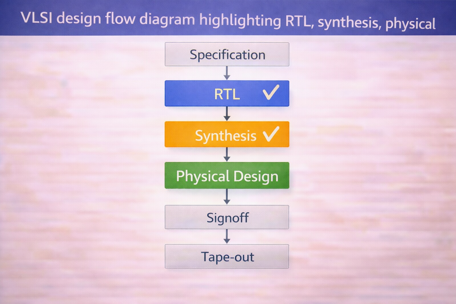
Typical VLSI Design Flow:
- Specification
- RTL Design
- Functional Verification
- Logic Synthesis
- Physical Design (Floorplan, Placement, Routing)
- Timing Closure
- Fabrication
RTL is the FIRST HARDWARE IMPLEMENTATION STEP
3. What is RTL (Register Transfer Level)?
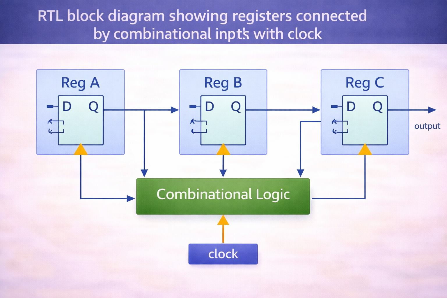
RTL describes how data moves between registers on a clock edge.
In simple words:
RTL tells what operation happens and when it happens with respect to clock
Example in plain English:
“At every rising edge of clock, add A and B and store the result in register C”
That sentence itself is RTL thinking.
Key words in RTL:
- Register
- Clock
- Transfer
- Combinational logic between registers
4. Why RTL is Needed (Very Important for Students)
Question:
Why not directly design transistor-level circuits?
Answer:
Because:
- Too complex
- Time-consuming
- Error-prone
- Not reusable
RTL provides:
- Abstraction
- Speed
- Reusability
- Technology independence
RTL code works for 28nm, 7nm, 5nm without change.
5. Why Verilog/SystemVerilog for RTL?
Verilog is:
- A Hardware Description Language (HDL)
- Used to describe hardware behavior and structure
Why NOT C / C++ / Python?
Software Language | HDL (Verilog) |
Executes line by line | Executes parallel |
Describes algorithm | Describes hardware |
No clock concept | Clock-based |
One CPU | Millions of gates |
Example Difference
C Code (Sequential)
a = b + c;
d = a + e;
Verilog (Parallel)
assign a = b + c;
assign d = a + e;
In hardware, both run at the same time.
6. Hardware Thinking vs Software Thinking
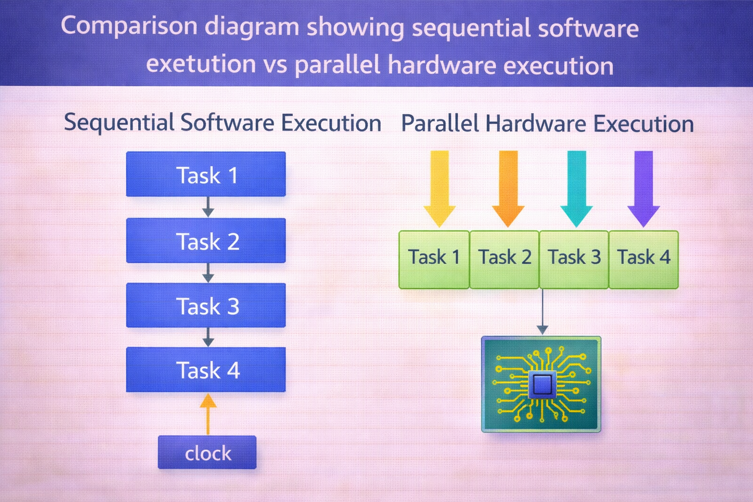
Software thinking:
- One instruction after another
- Single execution path
Hardware thinking:
- Everything happens at the same time
- Clock controls state updates
This is the biggest mental shift for students
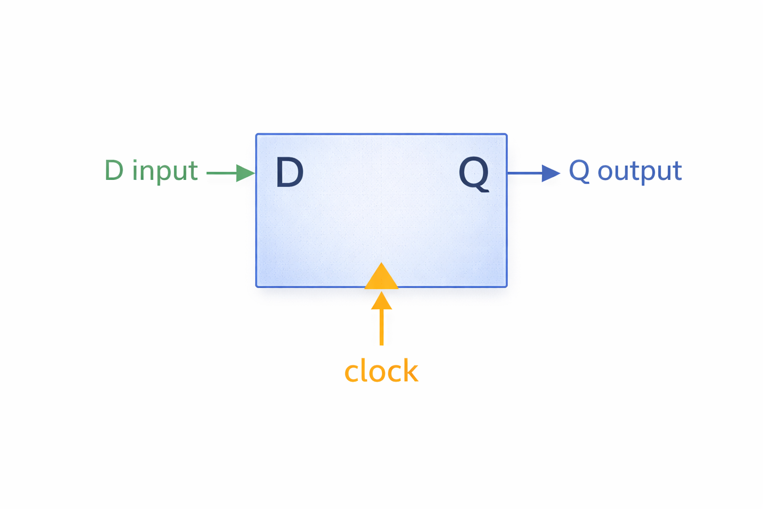
7. What is a Register?
A register:
- Stores 1 or more bits
- Updates only on clock edge
Example:
- D Flip-Flop stores 1 bit
- Register stores multiple bits
8. Combinational vs Sequential Logic (Foundation)
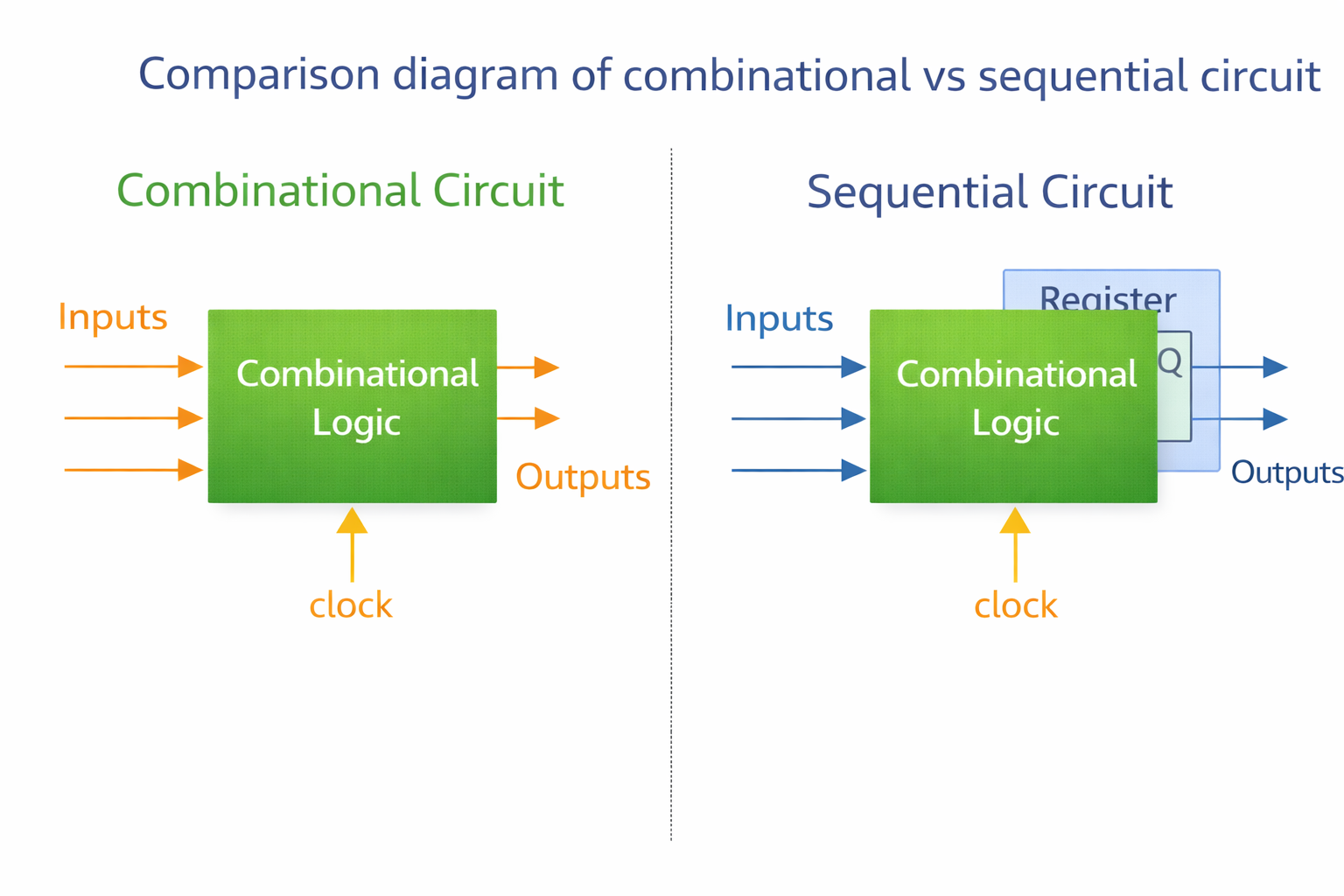
Combinational Logic
- Output depends ONLY on present input
- No memory
Examples:
- Adder
- MUX
- Decoder
Sequential Logic
- Output depends on:
- Present input
- Previous output (state)
- Has memory
Examples:
- Flip-flops
- Counters
- FSM
9. RTL Coding Styles (Overview – Will Deep Dive Later)
RTL can be written in three styles:
- Behavioral
- What the circuit does
- Dataflow
- Boolean equations
- Structural
- Gate-level connection
Same circuit → different RTL styles
10. What You Will Learn in This RTL Course (Assurance)
By the end, students will:
- Write clean synthesizable RTL
- Understand combinational & sequential circuits
- Code half adder → FSM
- Understand why PD engineers care about RTL
- Avoid common RTL mistakes
Class 1 Summary (For Students)
- RTL is heart of digital design
- Verilog is used to describe hardware
- Hardware ≠ software
- Everything is clock-driven
- This foundation is mandatory before PD
RTL DESIGN – CLASS 2
Verilog Basics | Module Structure | RTL Building Blocks
Level: Beginner
Goal: Student should confidently write and read basic RTL code
1. What is Verilog? (Clear Definition)
Verilog is a Hardware Description Language (HDL) used to:
- Describe digital hardware
- Model combinational and sequential circuits
- Simulate and synthesize real silicon hardware
Verilog does NOT describe software
Verilog describes how hardware behaves and connects
2. Structure of a Verilog Design
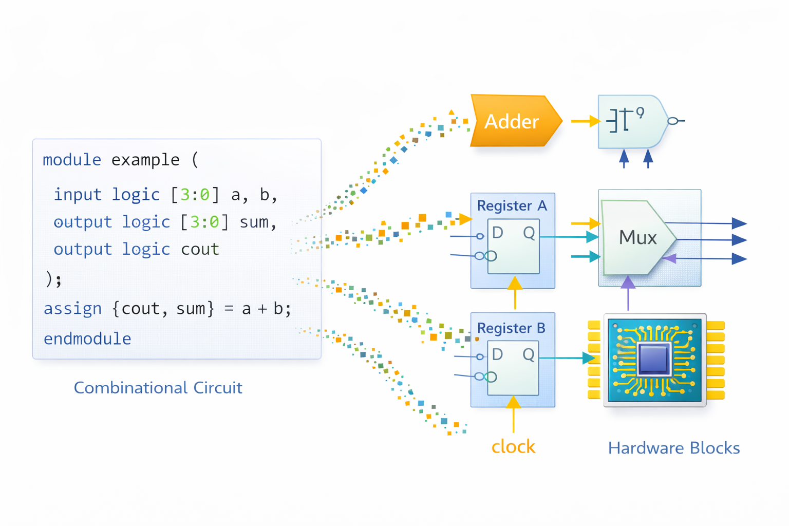
Every Verilog design is built using MODULES
Real-life analogy:
- Module = Black box
- Inputs → Processing → Outputs
3. Verilog Module Syntax (Very Important)
General Syntax:
module module_name (port_list);
// declarations
// logic
endmodule
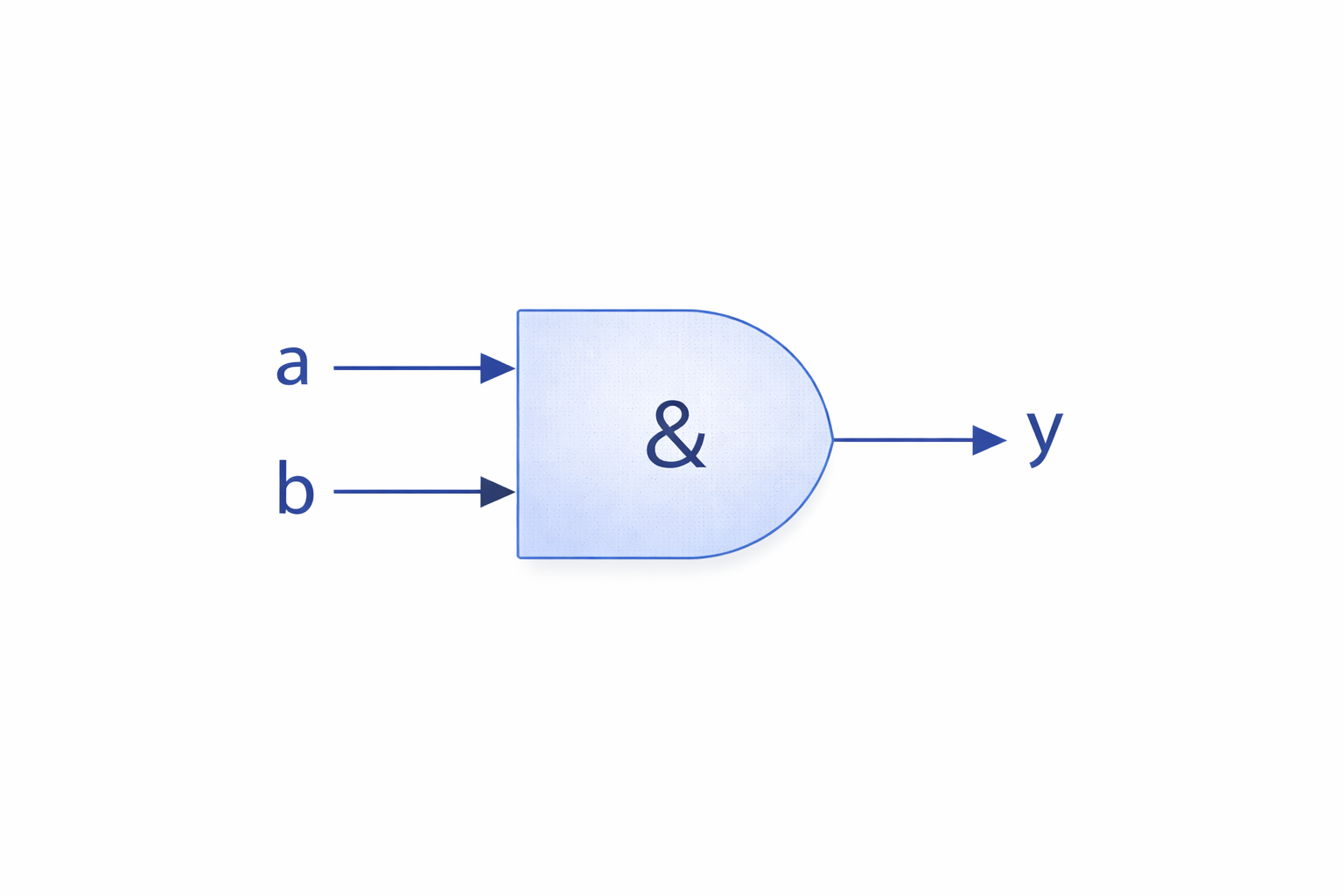
Example: Simple AND gate
module and_gate (
input a,
input b,
output y
);
assign y = a & b;
endmodule
Explanation:
- module and_gate → Name of the hardware block
- input a, b → Input pins
- output y → Output pin
- assign → Continuous assignment (combinational logic)
4. Ports in Verilog (Inputs & Outputs)
Types of Ports:
- input
- output
- inout (used rarely in RTL)
Example:
input clk;
input rst;
output out;
Inputs drive the module
Outputs are driven by the module
5. Data Types in Verilog (Critical for Beginners)
Main Data Types:
Type | Meaning |
wire | Used for combinational connections |
reg | Used to store values (inside always block) |
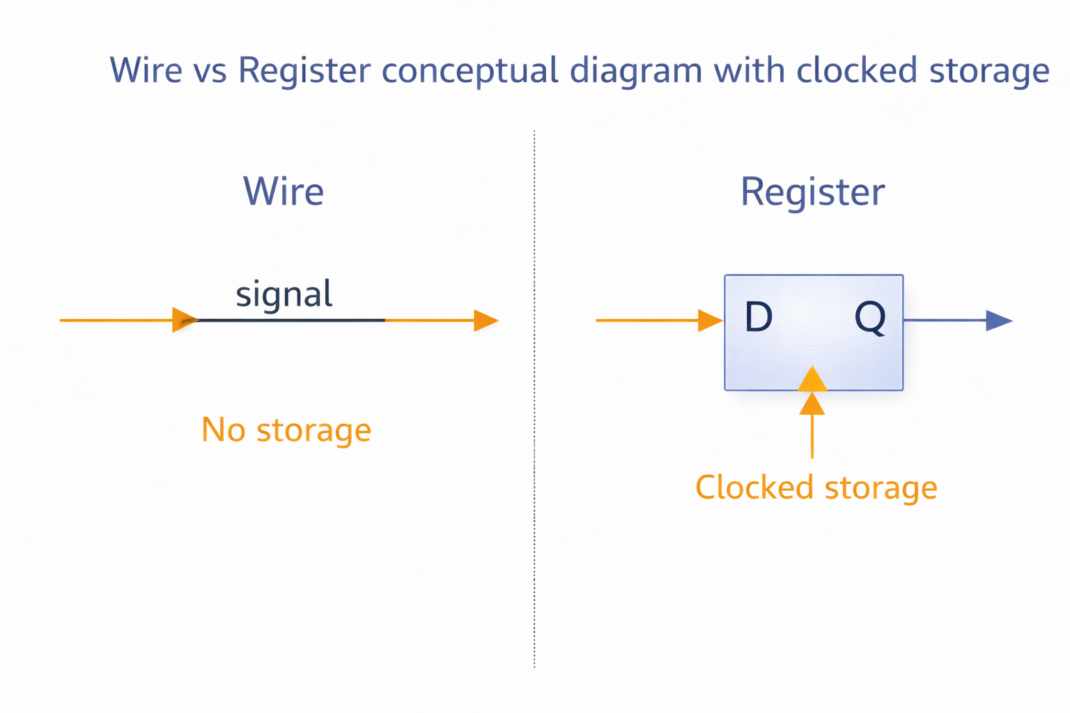
5.1 wire
- Represents physical wire
- Cannot store value
- Used with assign
wire sum;
assign sum = a ^ b;
5.2 reg
- Represents storage
- Used inside always blocks
- Holds value until changed
reg q;
always @(posedge clk)
q <= d;
reg does NOT mean register always
Depends on how it is coded
6. Continuous Assignment (assign)
Used for combinational logic
Syntax:
assign output = expression;
Example:
assign y = (a & b) | c;
Executes continuously
Hardware equivalent: logic gates
7. Always Block (Core of RTL)
Used for:
- Sequential logic
- Complex combinational logic
Syntax:
always @(sensitivity_list)
begin
// statements
end
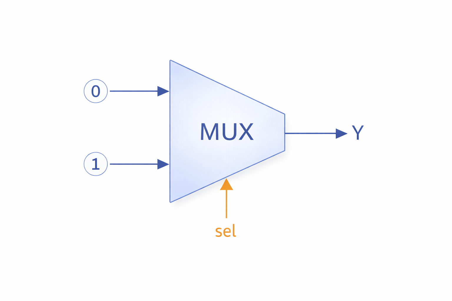
8. Combinational Always Block
Sensitivity List:
always @(*)
Example: 2:1 MUX
module mux2 (
input a,
input b,
input sel,
output reg y
);
always @(*) begin
if (sel)
y = b;
else
y = a;
end
endmodule
@(*) → All inputs automatically included
Use blocking assignment (=)
9. Sequential Always Block (Clocked Logic)
Syntax:
always @(posedge clk)
or
always @(negedge clk)
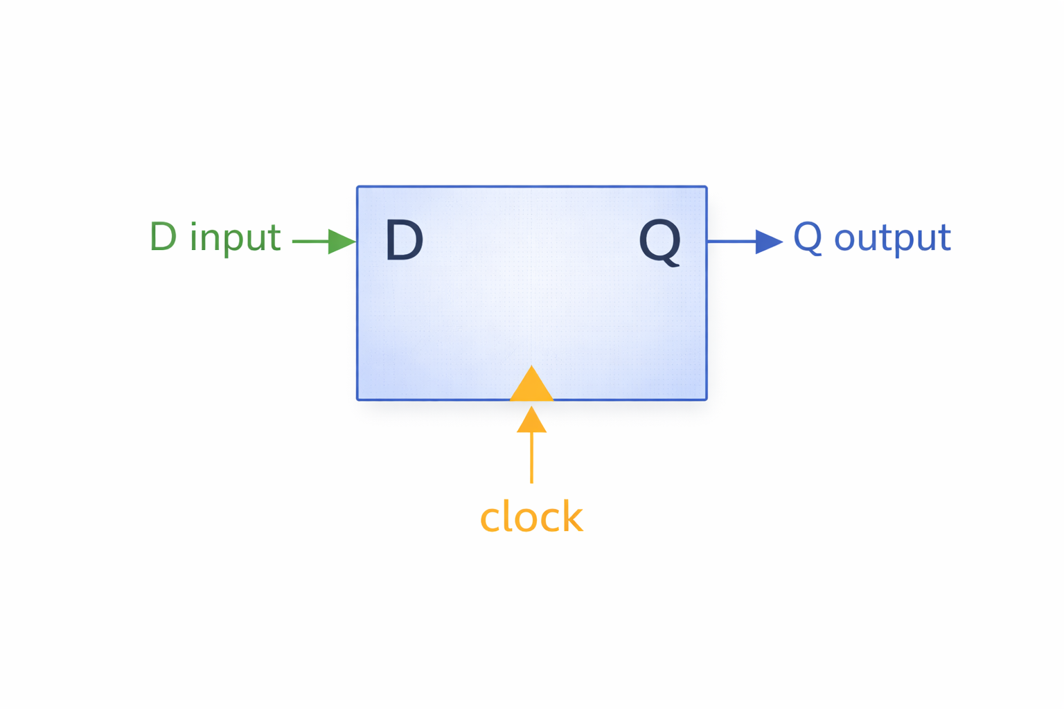
Example: D Flip-Flop
module dff (
input clk,
input d,
output reg q
);
always @(posedge clk) begin
q <= d;
end
endmodule
Use non-blocking assignment (<=)
Represents flip-flop
10. Blocking vs Non-Blocking Assignment (Very Important)
Blocking (=):
- Used in combinational
- Executes line by line
a = b;
c = a;
Non-blocking (<=):
- Used in sequential
- Executes in parallel
a <= b;
c <= a;
Golden Rule:
- Combinational → =
- Sequential → <=
11. Reset in Sequential Logic
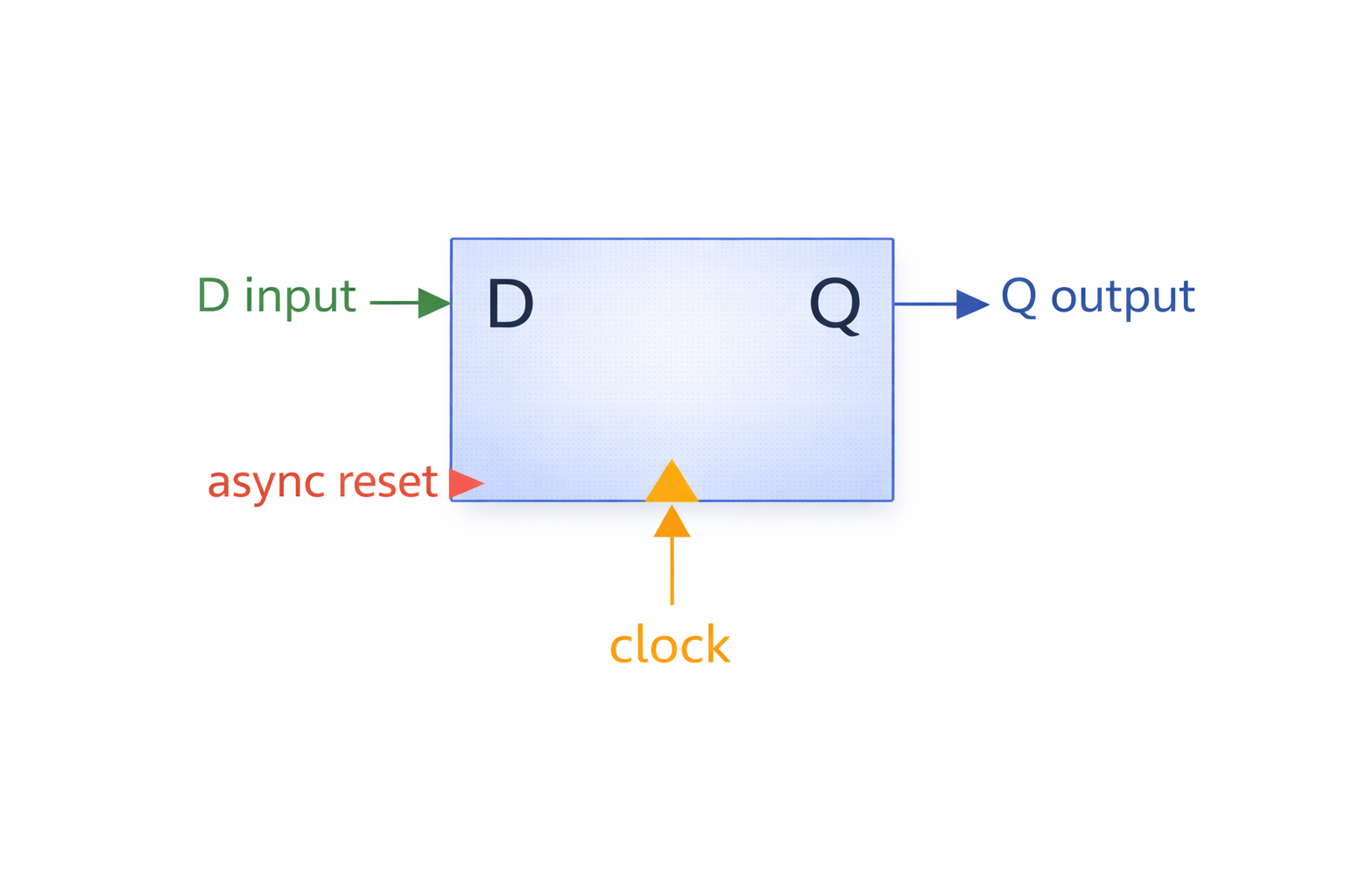
Asynchronous Reset
always @(posedge clk or posedge rst)
Example:
always @(posedge clk or posedge rst) begin
if (rst)
q <= 1'b0;
else
q <= d;
end
12. Simulation vs Synthesis (Must Understand)
Simulation:
- Verifies logic correctness
- Uses testbench
- No real hardware
Synthesis:
- Converts RTL → gates
- Used for chip fabrication
Some code simulates but does NOT synthesize
13. First RTL Design Flow
- Write RTL
- Compile
- Simulate
- Debug
- Synthesize
Class 2 Summary
✔ What is Verilog
✔ Module structure
✔ Inputs / Outputs
✔ wire vs reg
✔ assign
✔ always block
✔ combinational vs sequential
✔ blocking vs non-blocking
RTL DESIGN – CLASS 3
Combinational Circuits using Verilog RTL
Beginner Level
Goal: Student must be able to write, read, and understand RTL code for all basic combinational circuits
Coding Styles Covered:
✔ Behavioral
✔ Dataflow
✔ Structural
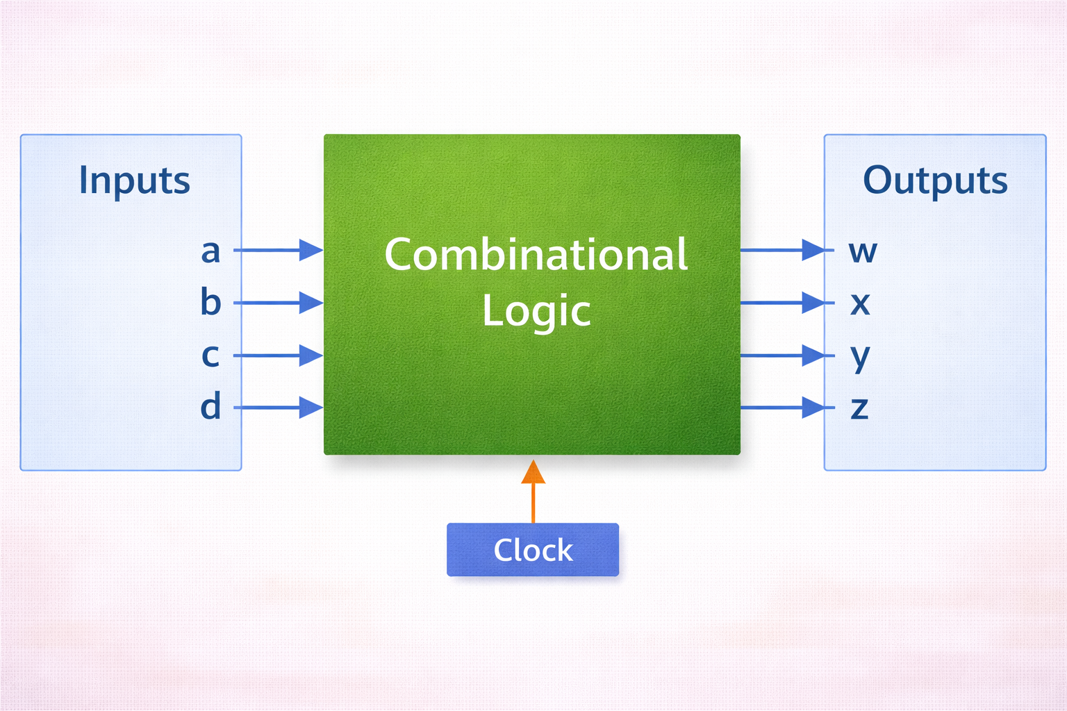
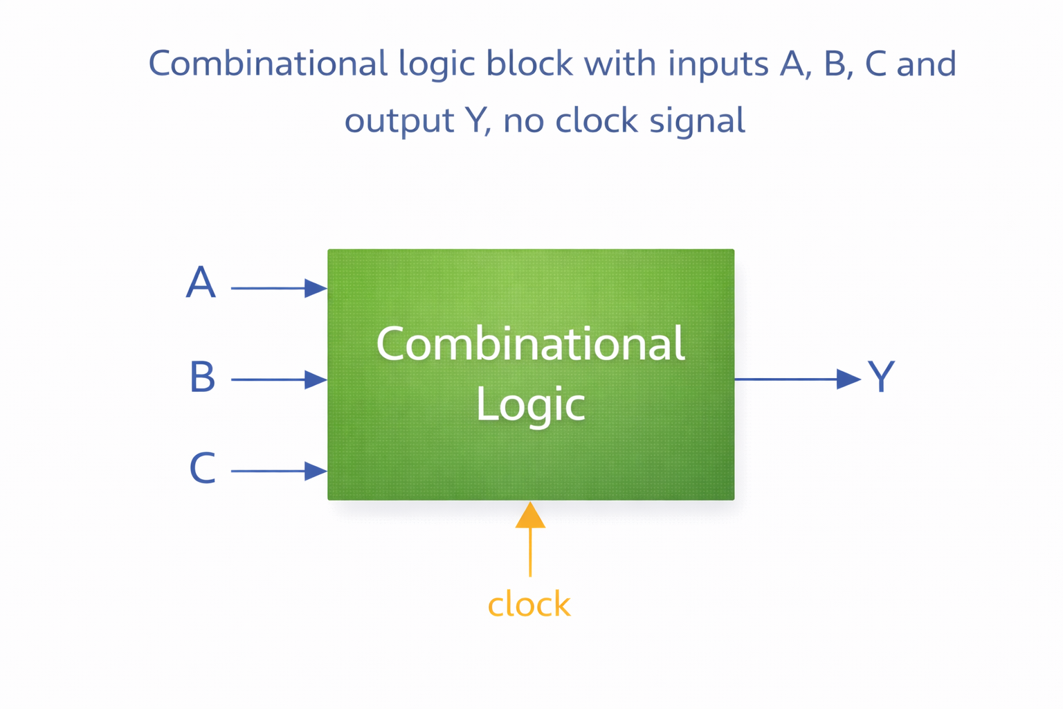
1. What is a Combinational Circuit?
Definition:
A combinational circuit is a digital circuit where:
- Output depends ONLY on present inputs
- No memory
- No clock
Example: Adder, MUX, Decoder, Encoder
2. Coding Styles in RTL (VERY IMPORTANT)
1️⃣ Behavioral Style
- Uses always @(*)
- High-level logic (if, case)
2️⃣ Dataflow Style
- Uses assign
- Boolean equations
3️⃣ Structural Style
- Gate-level modeling
- Uses AND, OR, XOR modules
Industry uses all three
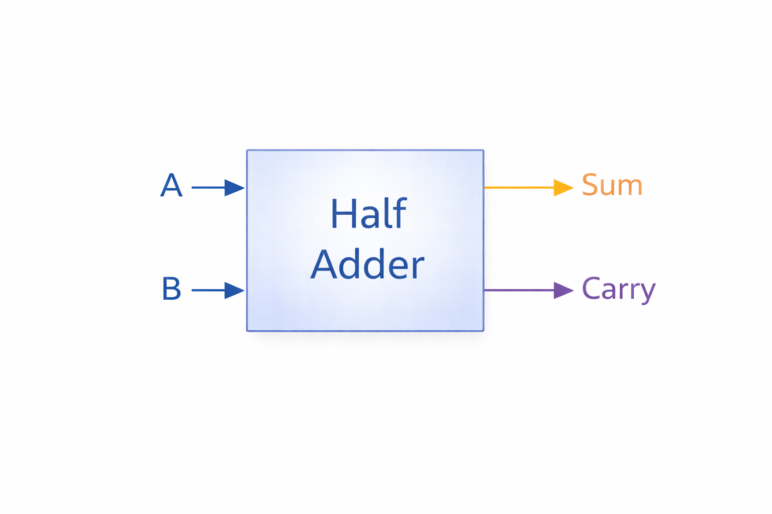
3. HALF ADDER
Function:
Adds two 1-bit numbers
A | B | Sum | Carry |
0 | 0 | 0 | 0 |
0 | 1 | 1 | 0 |
1 | 0 | 1 | 0 |
1 | 1 | 0 | 1 |
Boolean Expressions:
- Sum = A ⊕ B
- Carry = A · B
3.1 Half Adder – Dataflow Style
module half_adder_df (
input a,
input b,
output sum,
output carry
);
assign sum = a ^ b;
assign carry = a & b;
endmodule
3.2 Half Adder – Behavioral Style
module half_adder_beh (
input a,
input b,
output reg sum,
output reg carry
);
always @(*) begin
sum = a ^ b;
carry = a & b;
end
endmodule
3.3 Half Adder – Structural Style
module half_adder_struct (
input a,
input b,
output sum,
output carry
);
xor (sum, a, b);
and (carry, a, b);
endmodule
Structural = Gate-level
4. FULL ADDER
Function:
Adds 3 bits → A, B, Cin
A | B | Cin | Sum | Cout |
Boolean Expressions:
- Sum = A ⊕ B ⊕ Cin
- Cout = AB + BCin + ACin
4.1 Full Adder – Dataflow
module full_adder_df (
input a, b, cin,
output sum, cout
);
assign sum = a ^ b ^ cin;
assign cout = (a & b) | (b & cin) | (a & cin);
endmodule
4.2 Full Adder – Behavioral
module full_adder_beh (
input a, b, cin,
output reg sum, cout
);
always @(*) begin
sum = a ^ b ^ cin;
cout = (a & b) | (b & cin) | (a & cin);
end
endmodule
4.3 Full Adder – Structural (Using Half Adders)
module full_adder_struct (
input a, b, cin,
output sum, cout
);
wire s1, c1, c2;
half_adder_df ha1 (a, b, s1, c1);
half_adder_df ha2 (s1, cin, sum, c2);
assign cout = c1 | c2;
endmodule
This is VERY important for interviews
5. 2:1 MULTIPLEXER
Function:
Selects one input based on sel
Sel | Y |
0 | A |
1 | B |
5.1 MUX – Dataflow
assign y = sel ? b : a;
5.2 MUX – Behavioral
always @(*) begin
if (sel)
y = b;
else
y = a;
end
6. DECODER (2:4 Decoder)
Function:
Converts binary input → one-hot output
A1 | A0 | Y3 Y2 Y1 Y0 |
Decoder RTL
module decoder_2x4 (
input a1, a0,
output reg
);
always @(*) begin
y = 4'b0000;
case ({a1,a0})
2'b00: y = 4'b0001;
2'b01: y = 4'b0010;
2'b10: y = 4'b0100;
2'b11: y = 4'b1000;
endcase
end
endmodule
7. ENCODER (4:2 Encoder)
Function:
Reverse of decoder
Encoder RTL
module encoder_4x2 (
input
output reg
);
always @(*) begin
case (y)
4'b0001: a = 2'b00;
4'b0010: a = 2'b01;
4'b0100: a = 2'b10;
4'b1000: a = 2'b11;
default: a = 2'b00;
endcase
end
endmodule
8. MAGNITUDE COMPARATOR (1-bit)
Outputs:
- G → A > B
- E → A == B
- L → A < B
Comparator RTL
module comparator_1bit (
input a, b,
output g, e, l
);
assign g = a & ~b;
assign e = ~(a ^ b);
assign l = ~a & b;
endmodule
CLASS 3 SUMMARY
✔ Combinational logic
✔ 3 RTL coding styles
✔ Half Adder
✔ Full Adder
✔ MUX
✔ Decoder
✔ Encoder
✔ Comparator
RTL DESIGN – CLASS 4
Sequential Circuits using Verilog RTL (Beginner → Industry Ready)
Level: Beginner
Goal: Student must clearly understand memory, clock, flip-flops, and RTL coding
Focus:
✔ What makes sequential different
✔ All latches & flip-flops
✔ Proper RTL coding style (industry standard)
✔ Reset concepts
✔ Examples with explanation
1. What is a Sequential Circuit?
Definition:
A sequential circuit is a digital circuit where:
- Output depends on
Present input
Previous output (memory)
Memory is stored using latches and flip-flops
Key Difference
Feature | Combinational | Sequential |
Memory | No | Yes |
Clock | No | Yes |
Depends on past | No | Yes |
2. Clock – Heart of Sequential Logic
What is a Clock?
- A periodic signal (0 → 1 → 0)
- Controls when data is stored
Types:
- Positive edge (posedge)
- Negative edge (negedge)
Flip-flops work only on clock edge
3. Latch vs Flip-Flop (VERY IMPORTANT)
Feature | Latch | Flip-Flop |
Trigger | Level | Edge |
Clock | Enable | Clock |
Safe for RTL |
Industry uses Flip-Flops, not latches
4. SR LATCH (Basic Memory)
Function:
- Stores 1 bit
- Controlled by S (Set) and R (Reset)
S | R | Q |
0 | 0 | Hold |
1 | 0 | Set |
0 | 1 | Reset |
1 | 1 | Invalid |
SR Latch RTL (Behavioral)
module sr_latch (
input s, r,
output reg q
);
always @(*) begin
if (s && !r)
q = 1;
else if (!s && r)
q = 0;
end
endmodule
Avoid latch usage in real RTL
5. D LATCH
Why D Latch?
- Removes invalid condition
- Single input D
D Latch RTL
module d_latch (
input d, en,
output reg q
);
always @(*) begin
if (en)
q = d;
end
endmodule
Still level sensitive → not preferred
6. FLIP-FLOPS (MAIN FOCUS)
6.1 D Flip-Flop (MOST IMPORTANT)
Function:
- Stores data only on clock edge
Equation:
Q(t+1) = D
D Flip-Flop RTL (Industry Standard)
module d_ff (
input clk,
input d,
output reg q
);
always @(posedge clk) begin
q <= d;
end
endmodule
<= is non-blocking assignment (mandatory)
7. Reset in Flip-Flops
Why Reset?
- To initialize registers
- Prevent unknown (X) values
7.1 Asynchronous Reset
always @(posedge clk or posedge rst) begin
if (rst)
q <= 0;
else
q <= d;
end
✔ Reset works immediately
7.2 Synchronous Reset
always @(posedge clk) begin
if (rst)
q <= 0;
else
q <= d;
end
✔ Reset only on clock edge
Industry prefers synchronous reset
8. JK Flip-Flop
Function:
- No invalid state
- Toggle when J = K = 1
JK Flip-Flop RTL
module jk_ff (
input clk, j, k,
output reg q
);
always @(posedge clk) begin
case ({j,k})
2'b00: q <= q;
2'b01: q <= 0;
2'b10: q <= 1;
2'b11: q <= ~q;
endcase
end
endmodule
9. T Flip-Flop
Function:
- Toggle when T = 1
Equation:
Q(t+1) = Q ⊕ T
T Flip-Flop RTL
module t_ff (
input clk, t,
output reg q
);
always @(posedge clk) begin
if (t)
q <= ~q;
end
endmodule
Used in counters
10. SR Flip-Flop (Clocked)
module sr_ff (
input clk, s, r,
output reg q
);
always @(posedge clk) begin
if (s && !r)
q <= 1;
else if (!s && r)
q <= 0;
end
endmodule
11. Registers (Multiple Flip-Flops)
Example: 4-bit Register
module register_4bit (
input clk,
input
output reg
);
always @(posedge clk) begin
q <= d;
end
endmodule
Registers are everywhere in chips
12. Blocking vs Non-Blocking (INTERVIEW MUST)
Type | Symbol | Used in |
Blocking | = | Combinational |
Non-Blocking | <= | Sequential |
Wrong:
q = d;
Correct:
q <= d;
CLASS 4 SUMMARY
✔ Sequential logic concept
✔ Clock & memory
✔ Latches vs flip-flops
✔ D, JK, T, SR flip-flops
✔ Reset types
✔ Industry RTL style
RTL DESIGN – CLASS 5
Counters & Shift Registers using Verilog RTL
(All Sequential Circuits – Industry + Interview Ready)
1. What is a Counter?
Definition
A counter is a sequential circuit that:
- Counts clock pulses
- Changes output in a fixed sequence
Counters are built using flip-flops
2. Types of Counters
Type | Description |
Up Counter | Counts 0 → 15 |
Down Counter | Counts 15 → 0 |
Up-Down Counter | Both directions |
Mod-N Counter | Counts 0 → N-1 |
Ring Counter | Single 1 circulates |
Johnson Counter | Twisted ring |
3. 4-Bit UP Counter
Truth Example
0000 → 0001 → 0010 → 0011 → ... → 1111
RTL Code (Behavioral)
module up_counter (
input clk,
input rst,
output reg
);
always @(posedge clk) begin
if (rst)
count <= 4'b0000;
else
count <= count + 1;
end
endmodule
Explanation
- On reset → counter = 0
- Every clock → increment
4. 4-Bit DOWN Counter
module down_counter (
input clk,
input rst,
output reg
);
always @(posedge clk) begin
if (rst)
count <= 4'b1111;
else
count <= count - 1;
end
endmodule
Used in timers
5. UP-DOWN Counter
module up_down_counter (
input clk,
input rst,
input mode, // 1 = up, 0 = down
output reg
);
always @(posedge clk) begin
if (rst)
count <= 0;
else if (mode)
count <= count + 1;
else
count <= count - 1;
end
endmodule
6. MOD-N Counter (Example: MOD-10)
Why Mod Counter?
Used in:
- Digital clocks
- Frequency division
module mod10_counter (
input clk,
input rst,
output reg
);
always @(posedge clk) begin
if (rst || count == 9)
count <= 0;
else
count <= count + 1;
end
endmodule
7. Ring Counter
Definition
- Only one bit = 1
- Rotates each clock
0001 → 0010 → 0100 → 1000 → 0001
module ring_counter (
input clk,
input rst,
output reg
);
always @(posedge clk) begin
if (rst)
q <= 4'b0001;
else
q <= {q
end
endmodule
Used in FSM, control units
8. Johnson Counter
Definition
- Inverted feedback
0000 → 1000 → 1100 → 1110 → 1111 → 0111 → ...
module johnson_counter (
input clk,
input rst,
output reg
);
always @(posedge clk) begin
if (rst)
q <= 0;
else
q <= {~q
end
endmodule
9. Shift Registers
What is a Shift Register?
- Stores data
- Shifts left or right
10. Types of Shift Registers
Type | Meaning |
SISO | Serial In Serial Out |
SIPO | Serial In Parallel Out |
PISO | Parallel In Serial Out |
PIPO | Parallel In Parallel Out |
11. SISO Shift Register
module siso (
input clk,
input din,
output reg dout
);
reg
always @(posedge clk) begin
shift <= {shift
dout <= shift
end
endmodule
12. SIPO Shift Register
module sipo (
input clk,
input din,
output reg
);
always @(posedge clk) begin
q <= {q
end
endmodule
13. PISO Shift Register
module piso (
input clk,
input load,
input
output reg dout
);
reg
always @(posedge clk) begin
if (load)
temp <= din;
else begin
dout <= temp
temp <= temp >> 1;
end
end
endmodule
14. PIPO Shift Register
module pipo (
input clk,
input
output reg
);
always @(posedge clk) begin
q <= din;
end
endmodule
CLASS 5 SUMMARY
✔ All counter types
✔ Ring & Johnson counters
✔ Shift register types
✔ Clean RTL coding
✔ Reset handling
RTL DESIGN – CLASS 6
Finite State Machines (FSM) – COMPLETE BEGINNER TO INDUSTRY LEVEL
1. What is an FSM?
Definition
A Finite State Machine (FSM) is a sequential circuit that:
- Has a finite number of states
- Changes state based on:
- Present state
- Input
- Clock
FSM = Control Logic of SOC
2. Why FSM is Important in Industry?
FSM is used in:
- Traffic light controllers
- USB controllers
- Memory controllers
- Cache controllers
- Handshake logic
- Protocols (I2C, SPI, AXI)
90% of control logic = FSM
3. FSM Basic Blocks
+------------------+
| State Register | ← Clock
+------------------+
|
v
+------------------+
| Next State Logic |
+------------------+
|
v
+------------------+
| Output Logic |
+------------------+
4. Types of FSM
1️⃣ Moore Machine
- Output depends only on state
2️⃣ Mealy Machine
- Output depends on state + input
Feature | Moore | Mealy |
Output change | On clock | Immediately |
Speed | Slower | Faster |
Glitches | No | Possible |
Industry use | More | Less |
Moore FSM is preferred in RTL design
5. FSM Design Steps (VERY IMPORTANT)
Every FSM in industry follows these steps:
- Problem statement
- State diagram
- State table
- State encoding
- RTL coding
- Simulation
6. Example 1: Simple FSM (2-State Switch)
Problem
- Input = sw
- Output = led
- Toggle LED when switch = 1
State Diagram
OFF ----sw=1----> ON
ON ----sw=1----> OFF
7. RTL Coding Style for FSM (STANDARD STYLE)
Three Always Blocks (Industry Standard)
- State register
- Next state logic
- Output logic
8. FSM RTL Code (Moore FSM)
module simple_fsm (
input clk,
input rst,
input sw,
output reg led
);
typedef enum logic
state_t present_state, next_state;
/* State Register */
always @(posedge clk) begin
if (rst)
present_state <= OFF;
else
present_state <= next_state;
end
/* Next State Logic */
always @(*) begin
case (present_state)
OFF: if (sw) next_state = ON;
else next_state = OFF;
ON: if (sw) next_state = OFF;
else next_state = ON;
endcase
end
/* Output Logic */
always @(*) begin
case (present_state)
OFF: led = 0;
ON : led = 1;
endcase
end
endmodule
9. Example 2: Traffic Light Controller (Moore FSM)
States
- RED
- YELLOW
- GREEN
State Flow
RED → GREEN → YELLOW → RED
10. RTL Code: Traffic Light FSM
module traffic_light (
input clk,
input rst,
output reg red,
output reg yellow,
output reg green
);
typedef enum logic
state_t ps, ns;
/* State Register */
always @(posedge clk) begin
if (rst)
ps <= RED;
else
ps <= ns;
end
/* Next State Logic */
always @(*) begin
case (ps)
RED : ns = GREEN;
GREEN : ns = YELLOW;
YELLOW : ns = RED;
default: ns = RED;
endcase
end
/* Output Logic */
always @(*) begin
red = 0; yellow = 0; green = 0;
case (ps)
RED : red = 1;
GREEN : green = 1;
YELLOW : yellow = 1;
endcase
end
endmodule
11. Mealy FSM Example (Sequence Detector – 101)
Output becomes HIGH immediately
module seq_101 (
input clk,
input rst,
input in,
output reg out
);
typedef enum logic
state_t ps, ns;
always @(posedge clk)
if (rst) ps <= S0;
else ps <= ns;
always @(*) begin
out = 0;
case (ps)
S0: ns = in ? S1 : S0;
S1: ns = in ? S1 : S2;
S2: begin
if (in) begin
ns = S1;
out = 1;
end else ns = S0;
end
endcase
end
endmodule
12. Common FSM Mistakes (INTERVIEW)
Missing default case
Latch inference
Mixing blocking & non-blocking
No reset
Output in wrong always block
13. FSM Coding Best Practices
✔ Use typedef enum
✔ Separate always blocks
✔ Use non-blocking for registers
✔ Default assignments
✔ Reset logic mandatory
CLASS 6 SUMMARY
✔ FSM fundamentals
✔ Moore & Mealy
✔ Industry coding style
✔ Traffic light example
✔ Sequence detector
RTL DESIGN – CLASS 7
RTL Coding Guidelines, Simulation vs Synthesis & Timing-Safe Coding
(This class is CRITICAL for interviews + real project success)
1. Why RTL Coding Guidelines are IMPORTANT?
RTL code is written once, but it is:
- Simulated
- Synthesized
- Timed
- Placed & Routed
Bad RTL = Timing failure, latch inference, wrong silicon
2. Simulation vs Synthesis (MOST CONFUSING FOR BEGINNERS)
Simulation
- Software behavior check
- Uses event-based execution
- Accepts any logical code
Synthesis
- Converts RTL → Gates
- Hardware realization
- Only synthesizable constructs allowed
Feature | Simulation | Synthesis |
Purpose | Verify logic | Build hardware |
Executes | Sequentially | Parallel hardware |
Delays | #10 allowed | Not allowed |
Loops | Any | Must be bounded |
Wrong (Simulation only)
#10 a = b;
Correct (Synthesizable)
always @(posedge clk)
a <= b;
3. Blocking vs Non-Blocking Assignments
Blocking (=)
- Executes line by line
- Used for combinational logic
Non-Blocking (<=)
- Executes in parallel
- Used for sequential logic
Wrong Coding
always @(posedge clk) begin
a = b;
c = a;
end
Correct Coding
always @(posedge clk) begin
a <= b;
c <= a;
end
Rule (INTERVIEW QUESTION)
Sequential → Non-blocking
Combinational → Blocking
4. Latch vs Flip-Flop (VERY IMPORTANT)
Latch
- Level sensitive
- Enable based
- Unintentional → BAD
Flip-Flop
- Edge triggered
- Clock based
- Preferred
Latch Inference (BAD)
always @(*) begin
if (en)
q = d;
end
➡ When en=0, q holds value → latch inferred
Flip-Flop Coding
always @(posedge clk) begin
if (en)
q <= d;
end
5. How Latches are Accidentally Created
Missing else
Incomplete case
No default assignment
Wrong
always @(*) begin
if (a)
y = b;
end
Correct
always @(*) begin
y = 0;
if (a)
y = b;
end
6. Reset Types in RTL
1️⃣ Synchronous Reset
- Works with clock
- Preferred for timing
always @(posedge clk) begin
if (rst)
q <= 0;
else
q <= d;
end
2️⃣ Asynchronous Reset
- Immediate reset
- Used for power-on
always @(posedge clk or negedge rst_n) begin
if (!rst_n)
q <= 0;
else
q <= d;
end
7. Clock Gating (POWER SAVING CONCEPT)
Why?
- Reduce dynamic power
- Used in SOCs
Wrong (Manual gating)
always @(posedge clk & en)
This causes clock glitches
Correct (Enable based)
always @(posedge clk) begin
if (en)
q <= d;
end
Clock gating is done by tools, not RTL designer
8. Combinational Logic Coding Rules
Correct Template
always @(*) begin
y = 0;
case (sel)
2'b00: y = a;
2'b01: y = b;
2'b10: y = c;
2'b11: y = d;
endcase
end
✔ Default assignment
✔ Full coverage
9. Sequential Logic Coding Rules
Correct Template
always @(posedge clk) begin
if (rst)
q <= 0;
else
q <= d;
end
✔ Non-blocking
✔ Reset included
10. Sensitivity List (Beginner Mistake)
Wrong
always @(a)
Correct
always @(*)
Avoid missing signals
11. Timing Concepts (Beginner Level)
Setup Time
- Data stable before clock
Hold Time
- Data stable after clock
Bad RTL → setup/hold violations
12. Interview-Level RTL Rules
✔ One clock per always block
✔ No delays #
✔ No initial block (except testbench)
✔ Avoid combinational loops
✔ Use parameters
CLASS 7 SUMMARY
✔ Simulation vs Synthesis
✔ Blocking vs Non-blocking
✔ Latch avoidance
✔ Reset handling
✔ Timing-safe RTL
RTL DESIGN – CLASS 8
Combinational Circuits using RTL (Behavioral, Dataflow & Structural)
This class is the FOUNDATION of RTL
Every VLSI student must know these circuits in RTL
1. What is a Combinational Circuit?
A combinational circuit:
- Output depends only on present inputs
- No memory
- No clock
Examples:
- Adder
- Subtractor
- MUX
- Decoder
- Encoder
- Comparator
2. RTL Coding Styles (VERY IMPORTANT)
There are 3 ways to write RTL code:
Style | Description | Usage |
Behavioral | Uses always block | Most common |
Dataflow | Uses assign statement | Simple logic |
Structural | Uses gates/modules | Low-level |
All three generate same hardware
3. HALF ADDER
Function
Adds two 1-bit numbers
A | B | Sum | Carry |
0 | 0 | 0 | 0 |
0 | 1 | 1 | 0 |
1 | 0 | 1 | 0 |
1 | 1 | 0 | 1 |
Equations
Sum = A ^ B
Carry = A & B
3.1 Half Adder – Dataflow Style
module half_adder_df (
input A, B,
output Sum, Carry
);
assign Sum = A ^ B;
assign Carry = A & B;
endmodule
3.2 Half Adder – Behavioral Style
module half_adder_beh (
input A, B,
output reg Sum, Carry
);
always @(*) begin
Sum = A ^ B;
Carry = A & B;
end
endmodule
3.3 Half Adder – Structural Style
module half_adder_str (
input A, B,
output Sum, Carry
);
xor (Sum, A, B);
and (Carry, A, B);
endmodule
4. FULL ADDER
Function
Adds 3 inputs: A, B, Cin
A | B | Cin | Sum | Cout |
Equations
Sum = A ^ B ^ Cin
Cout = (A&B) | (B&Cin) | (A&Cin)
4.1 Full Adder – Dataflow
module full_adder_df (
input A, B, Cin,
output Sum, Cout
);
assign Sum = A ^ B ^ Cin;
assign Cout = (A & B) | (B & Cin) | (A & Cin);
endmodule
4.2 Full Adder – Behavioral
module full_adder_beh (
input A, B, Cin,
output reg Sum, Cout
);
always @(*) begin
Sum = A ^ B ^ Cin;
Cout = (A & B) | (B & Cin) | (A & Cin);
end
endmodule
4.3 Full Adder – Structural (Using Half Adders)
module full_adder_str (
input A, B, Cin,
output Sum, Cout
);
wire s1, c1, c2;
xor (s1, A, B);
and (c1, A, B);
xor (Sum, s1, Cin);
and (c2, s1, Cin);
or (Cout, c1, c2);
endmodule
5. RIPPLE CARRY ADDER (4-bit)
Multiple full adders connected in series
5.1 4-bit Ripple Carry Adder – Behavioral
module rca_4bit (
input
input Cin,
output
output Cout
);
assign {Cout, Sum} = A + B + Cin;
endmodule
✔ Best synthesizable
✔ Industry preferred
6. MULTIPLEXER (2:1 MUX)
Function
Selects one input based on select line
S | Y |
0 | A |
1 | B |
6.1 MUX – Dataflow
module mux2_df (
input A, B, S,
output Y
);
assign Y = S ? B : A;
endmodule
6.2 MUX – Behavioral
module mux2_beh (
input A, B, S,
output reg Y
);
always @(*) begin
if (S)
Y = B;
else
Y = A;
end
endmodule
6.3 MUX – Structural
module mux2_str (
input A, B, S,
output Y
);
wire sbar, w1, w2;
not (sbar, S);
and (w1, A, sbar);
and (w2, B, S);
or (Y, w1, w2);
endmodule
7. DECODER (2:4)
Function
One output HIGH based on input
7.1 Decoder – Behavioral
module decoder2to4 (
input
output reg
);
always @(*) begin
Y = 4'b0000;
case (A)
2'b00: Y = 4'b0001;
2'b01: Y = 4'b0010;
2'b10: Y = 4'b0100;
2'b11: Y = 4'b1000;
endcase
end
endmodule
8. ENCODER (4:2)
module encoder4to2 (
input
output reg
);
always @(*) begin
case (Y)
4'b0001: A = 2'b00;
4'b0010: A = 2'b01;
4'b0100: A = 2'b10;
4'b1000: A = 2'b11;
default: A = 2'b00;
endcase
end
endmodule
9. MAGNITUDE COMPARATOR (1-bit)
module comparator_1bit (
input A, B,
output A_gt_B, A_eq_B, A_lt_B
);
assign A_gt_B = A & ~B;
assign A_eq_B = ~(A ^ B);
assign A_lt_B = ~A & B;
endmodule
CLASS 8 SUMMARY
✔ Half Adder
✔ Full Adder
✔ Ripple Carry Adder
✔ MUX
✔ Decoder
✔ Encoder
✔ Comparator
✔ All 3 RTL styles
RTL DESIGN – CLASS 9
SEQUENTIAL CIRCUITS USING RTL (COMPLETE BEGINNER → INDUSTRY LEVEL)
1. What is a Sequential Circuit?
A sequential circuit is a digital circuit where:
Output depends on
- Present inputs
- Previous output (stored state)
Memory is required
Clock signal is mandatory
🔁 Difference Recap
Combinational | Sequential |
No memory | Has memory |
No clock | Clock required |
Depends only on inputs | Depends on inputs + past |
Example: Adder | Example: Flip-Flop |
2. Memory Element in RTL
Memory is implemented using:
- Latch
- Flip-Flop
In RTL:
- always block
- posedge / negedge clock
- non-blocking assignment (<=)
3. Why Non-Blocking Assignment (<=)?
Wrong for Sequential
Q = D;
Correct for Sequential
Q <= D;
Ensures:
- Proper clocked behavior
- No race conditions
4. LATCH vs FLIP-FLOP (RTL VIEW)
Latch | Flip-Flop |
Level sensitive | Edge sensitive |
No clock edge | Clock edge |
Unsafe for RTL | Preferred in RTL |
Industry Rule:
Avoid latches
Use flip-flops only
5. SR FLIP-FLOP (RTL)
Function:
- S = Set
- R = Reset
Truth Table
S | R | Q(next) |
0 | 0 | Hold |
0 | 1 | 0 |
1 | 0 | 1 |
1 | 1 | Invalid |
RTL Code (Behavioral)
module sr_ff (
input clk,
input S, R,
output reg Q
);
always @(posedge clk) begin
if (S && !R)
Q <= 1;
else if (!S && R)
Q <= 0;
else if (!S && !R)
Q <= Q; // hold
end
endmodule
S=R=1 is avoided
6. D FLIP-FLOP (MOST IMPORTANT)
Why D FF is MOST USED?
✔ No invalid state
✔ Simple
✔ Safe
✔ Used in registers, pipelines
Function
Q(next) = D
RTL – D Flip-Flop
module d_ff (
input clk,
input D,
output reg Q
);
always @(posedge clk) begin
Q <= D;
end
endmodule
D FF with Reset (Industry Standard)
module d_ff_reset (
input clk,
input rst,
input D,
output reg Q
);
always @(posedge clk) begin
if (rst)
Q <= 0;
else
Q <= D;
end
endmodule
7. JK FLIP-FLOP
Function:
J | K | Action |
0 | 0 | Hold |
0 | 1 | Reset |
1 | 0 | Set |
1 | 1 | Toggle |
RTL Code
module jk_ff (
input clk,
input J, K,
output reg Q
);
always @(posedge clk) begin
case ({J,K})
2'b00: Q <= Q;
2'b01: Q <= 0;
2'b10: Q <= 1;
2'b11: Q <= ~Q;
endcase
end
endmodule
8. T FLIP-FLOP
Function:
T | Q(next) |
0 | Hold |
1 | Toggle |
RTL Code
module t_ff (
input clk,
input T,
output reg Q
);
always @(posedge clk) begin
if (T)
Q <= ~Q;
else
Q <= Q;
end
endmodule
9. REGISTER (4-BIT)
Register = Collection of flip-flops
RTL Code
module reg_4bit (
input clk,
input
output reg
);
always @(posedge clk) begin
Q <= D;
end
endmodule
10. SHIFT REGISTER
Types:
- SISO
- SIPO
- PISO
- PIPO
Example: 4-bit Shift Right Register
module shift_reg (
input clk,
input D,
output reg
);
always @(posedge clk) begin
Q <= {D, Q
end
endmodule
11. COUNTERS
11.1 UP COUNTER (4-BIT)
module up_counter (
input clk,
input rst,
output reg
);
always @(posedge clk) begin
if (rst)
count <= 0;
else
count <= count + 1;
end
endmodule
11.2 DOWN COUNTER
count <= count - 1;
12. SYNCHRONOUS vs ASYNCHRONOUS RESET
Synchronous Reset
always @(posedge clk)
Asynchronous Reset
always @(posedge clk or posedge rst)
13. COMMON RTL INTERVIEW RULES
Use always @(posedge clk)
Use <= for sequential
Never mix blocking and non-blocking
Avoid latches
Avoid delays #10
CLASS 9 COMPLETE
✔ All Flip-Flops
✔ Registers
✔ Counters
✔ Shift Registers
✔ Industry RTL Rules
RTL DESIGN – CLASS 10
FINITE STATE MACHINES (FSM) + REAL RTL MINI PROJECTS
This class is EXTREMELY IMPORTANT for
RTL Design
Physical Design
Interviews
Industry projects
1. What is an FSM (Finite State Machine)?
An FSM is a sequential circuit that:
- Has finite number of states
- Changes state on clock edge
- Output depends on:
- Present state
- Inputs
FSM Components
- State Register (Flip-Flops)
- Next State Logic
- Output Logic
- Clock + Reset
2. Types of FSM
🔹 Moore Machine
- Output depends only on state
🔹 Mealy Machine
- Output depends on state + input
Comparison Table
Feature | Moore | Mealy |
Output depends on | State | State + Input |
Output changes | On clock | Immediately |
Safe | Yes | Risky |
Industry usage | HIGH | MEDIUM |
Industry prefers MOORE FSM
3. FSM DESIGN FLOW (VERY IMPORTANT)
1️⃣ Write Problem Statement
2️⃣ Draw State Diagram
3️⃣ Create State Table
4️⃣ Assign Binary Encoding
5️⃣ Write RTL Code
6️⃣ Simulate
7️⃣ Synthesize
4. FSM EXAMPLE 1 – SIMPLE TOGGLE FSM
Problem:
- Output toggles every clock
State Diagram
- S0 → Q=0
- S1 → Q=1
RTL Code (Moore FSM)
module toggle_fsm (
input clk,
input rst,
output reg out
);
typedef enum logic
state_t state, next_state;
always @(posedge clk) begin
if (rst)
state <= S0;
else
state <= next_state;
end
always @(*) begin
case (state)
S0: next_state = S1;
S1: next_state = S0;
endcase
end
always @(*) begin
case (state)
S0: out = 0;
S1: out = 1;
endcase
end
endmodule
5. FSM EXAMPLE 2 – SEQUENCE DETECTOR (101)
Problem:
- Detect input sequence 101
- Output = 1 when detected
States
- S0 → Start
- S1 → Got 1
- S2 → Got 10
RTL Code
module seq_101 (
input clk,
input rst,
input in,
output reg out
);
typedef enum logic
state_t state, next;
always @(posedge clk) begin
if (rst)
state <= S0;
else
state <= next;
end
always @(*) begin
case (state)
S0: next = in ? S1 : S0;
S1: next = in ? S1 : S2;
S2: next = in ? S1 : S0;
endcase
end
always @(*) begin
out = (state == S2 && in);
end
endmodule
6. FSM EXAMPLE 3 – TRAFFIC LIGHT CONTROLLER
States
- RED
- GREEN
- YELLOW
RTL Code
module traffic_fsm (
input clk,
input rst,
output reg
);
typedef enum logic
state_t state, next;
always @(posedge clk) begin
if (rst)
state <= RED;
else
state <= next;
end
always @(*) begin
case (state)
RED: next = GREEN;
GREEN: next = YELLOW;
YELLOW: next = RED;
endcase
end
always @(*) begin
case (state)
RED: light = 3'b100;
GREEN: light = 3'b010;
YELLOW: light = 3'b001;
endcase
end
endmodule
7. RTL MINI PROJECT 1 – HALF ADDER
Behavioral
module half_adder (
input A, B,
output SUM, CARRY
);
assign SUM = A ^ B;
assign CARRY = A & B;
endmodule
8. RTL MINI PROJECT 2 – FULL ADDER
Dataflow
module full_adder (
input A, B, Cin,
output SUM, Cout
);
assign SUM = A ^ B ^ Cin;
assign Cout = (A & B) | (B & Cin) | (A & Cin);
endmodule
9. Behavioral vs Structural vs Dataflow (RECAP)
Style | Used For |
Behavioral | FSM, Counters |
Dataflow | Combinational |
Structural | Gate-level |
10. INDUSTRY CODING RULES (VERY IMPORTANT)
✔ One always block = one purpose
✔ FSM → 3 always blocks
✔ Use parameters / enum
✔ Reset mandatory
✔ No delays
✔ No latches