Module 1
Introduction to Electronics
Topics Covered
Basic Electronics: From Materials to Energy Bands (Lecture-Style Explanation)
Introduction
Today, we are going to discuss Basic Electronics. When we hear the word electronics, many students immediately think about circuits, wires, and devices. But before reaching that stage, we must clearly understand materials and their internal structure.
In Basic Electronics, we mainly classify materials into three types:
- Conductors
- Semiconductors
- Insulators
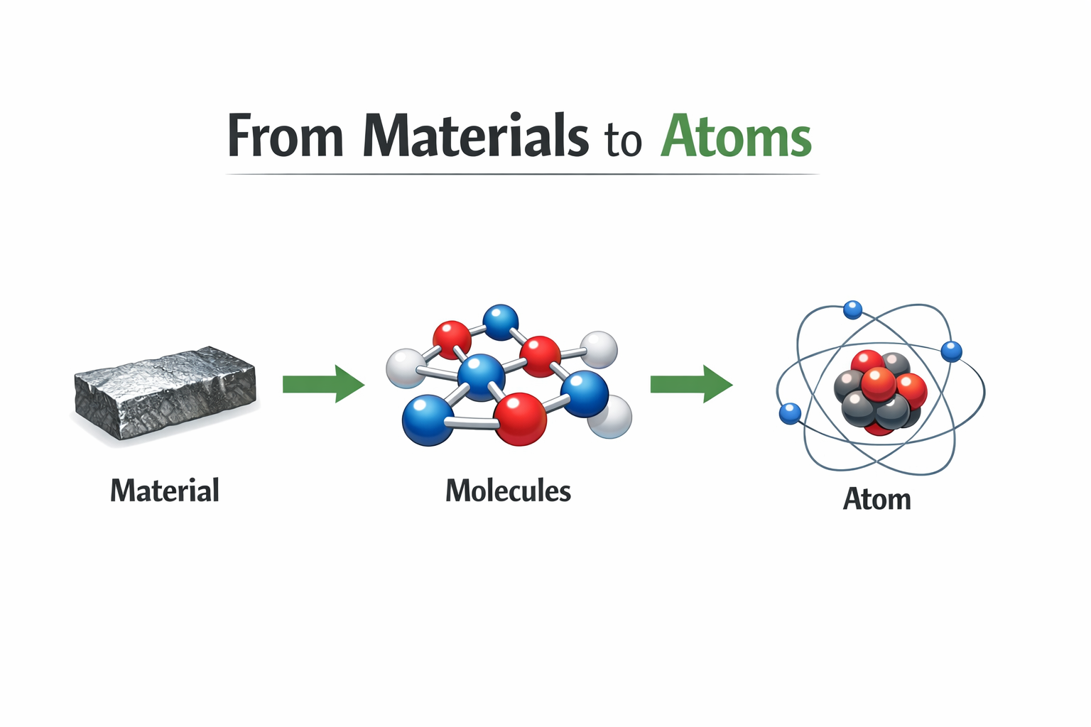
To understand why materials behave differently, we must go deep—from materials to molecules, from molecules to atoms, and finally into the internal structure of the atom.
What Is a Material?
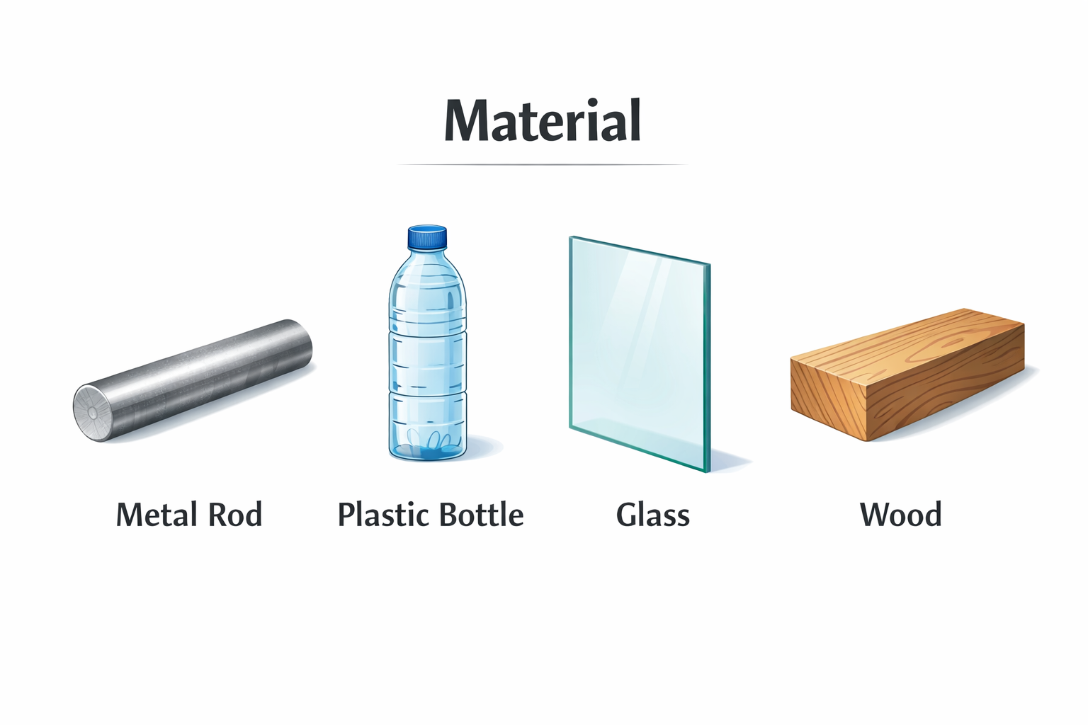
A material is anything that exists physically in this world. If you observe carefully:
- Objects around us are materials
- The human body is also made of material
- Solid, liquid, and gaseous substances are all materials
Every object we see is made using some material. These materials are not continuous; they are made up of molecules.
The physical state of a material—solid, liquid, or gas—depends on how its molecules are arranged and how strongly they are bonded.
Molecules and Atoms
A molecule is a group of atoms bonded together. Molecules are the basic units that decide the properties of a material.
When we go deeper, we find that:
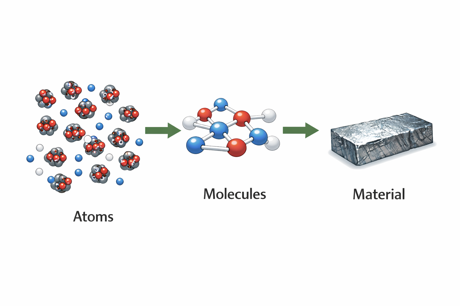
- Molecules are made up of atoms
- Atoms are the fundamental building blocks of matter
Millions of atoms together form a molecule, and millions of molecules together form a material.
Structure of an Atom
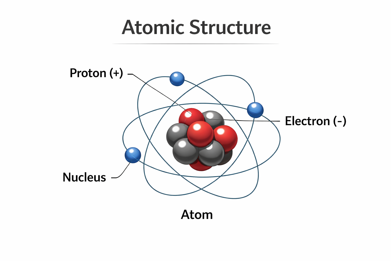
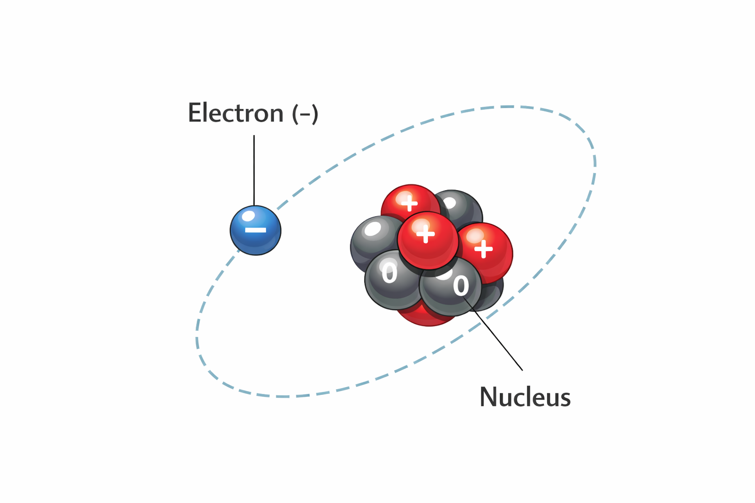
An atom is not a solid particle; it has its own internal structure. Every atom consists of two main parts:
1. Nucleus
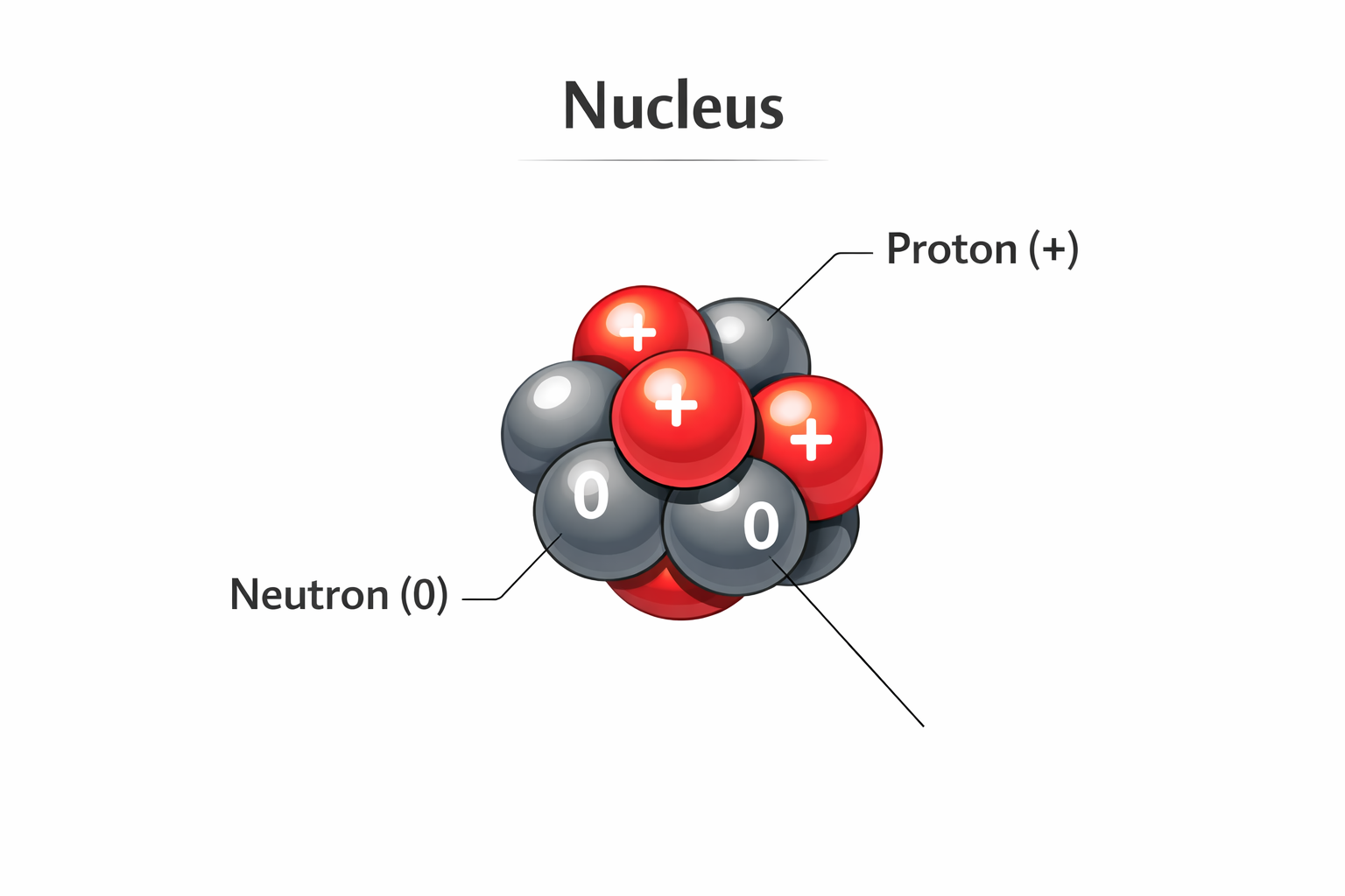
The nucleus is the central core of the atom. Inside the nucleus, we have:
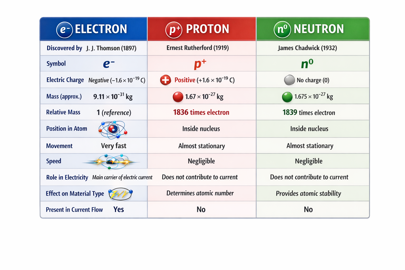
- Protons → positively charged particles
- Neutrons → particles with no charge
The nucleus contains almost all the mass of the atom.
2. Electrons
Outside the nucleus, electrons revolve around it in circular paths or energy levels.
- Electrons carry negative charge
- They are very small and very light
An atom is formed by the combination of:
Protons and neutrons inside the nucleus, and electrons revolving around the nucleus.
From Atomic Structure to Basic Electronics
Now let us connect atomic structure to Basic Electronics.
The behavior of a material in electronics depends mainly on electrons, especially the electrons present in the outermost shell of the atom.
To understand this clearly, we need to learn some important terms.
Important Terms in Basic Electronics
Valence Electron
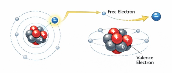
The electron that revolves around the nucleus and is under the control of the nucleus is called a Valence Electron.
- These electrons are present in the outermost shell
- They are involved in bonding
- We say they are in the Valence Band
Free Electron
If a valence electron comes out of the control of the nucleus, it becomes a Free Electron.
- A free electron can move freely inside the material
- It is responsible for the flow of electric current
Conduction Band
When an electron becomes a free electron, we say it has moved into the Conduction Band.
Energy Band Theory
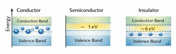
The difference between the Valence Band and the Conduction Band is called the Energy Gap.
This energy gap plays a very important role in deciding whether a material behaves as a conductor, semiconductor, or insulator.
The energy gap is measured in electron volts (eV).
Classification of Materials Based on Energy Bands
1. Conductors
In conductors, the Valence Band and Conduction Band overlap.
- There is no energy gap
- Electrons are already free
- No external energy is required to move electrons
Because conductors have a large number of free electrons:
- They conduct electricity very easily
Examples: Copper, Aluminum, Silver
Semiconductors
In semiconductors, the energy gap between the valence band and conduction band is approximately 1 eV.
Important point:
- This gap is not a physical gap, it is an energy gap
For a valence electron to become a free electron:
- We must apply an external energy of about 1 eV
So:
- Without external energy → it behaves like an insulator
- With external energy → it behaves like a conductor
That is why this material is called a semiconductor.
Examples: Silicon, Germanium
Insulators
In insulators, the energy gap between the valence band and conduction band is very large—approximately 6 eV.
- A very high external energy is required
- Normally, we do not apply such high energy
As a result:
- Electrons remain tightly bound
- No electric current flows
Examples: Rubber, Glass, Plastic, Wood
1. Electric Current
Definition
Electric current is defined as the rate of flow of electric charge through a conductor. In metallic conductors, this flow is mainly due to the movement of free electrons.
In simple terms, current tells us how much charge flows per second through a wire.
Mathematical Expression
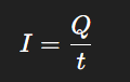
Where:
I = Electric current
Q = Electric charge
t = Time
Unit
- Ampere (A)
One ampere is defined as the flow of one coulomb of charge per second.
Important Points
- Current flows from higher potential to lower potential (conventional current direction).
- Electron flow is in the opposite direction to conventional current.
- Current can be DC (Direct Current) or AC (Alternating Current).
2. Electric Voltage
Definition
Electric voltage, also called electric potential difference, is the energy required to move a unit charge from one point to another in an electric circuit.
Voltage can be understood as the driving force that causes current to flow.
Mathematical Expression
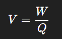
Where:
V = Voltage
W = Electrical work done
Q = Charge
Unit
- Volt (V)
One volt is the potential difference when one joule of energy is used to move one coulomb of charge.
Important Points
- Voltage does not flow; it exists between two points.
- A voltage source (battery or supply) is required to maintain current flow.
- Without voltage, no current can flow in a circuit.
3. Electric Power
Definition
Electric power is the rate at which electrical energy is converted into other forms of energy, such as heat, light, or mechanical energy.
Mathematical Expression
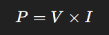
Where:
P = Power
V = Voltage
I = Current
Unit
- Watt (W)
One watt is the power consumed when one volt causes one ampere of current to flow.
Alternate Forms
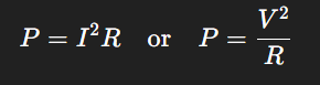
Using Ohm’s Law (introduced later), power can also be written as:
Important Points
- Electrical devices are rated in terms of power (e.g., 60 W bulb).
- Higher power means greater energy consumption per unit time.
4. Relationship Between Current, Voltage, and Power
- Voltage provides the force that pushes charges.
- Current represents the flow of charges.
- Power indicates how fast electrical energy is being used.
These three quantities are interdependent, and understanding their relationship is essential for circuit analysis.
Ohm’s Law
Ohm’s Law is one of the most fundamental principles in electronics. It states that the voltage across a resistor is directly proportional to the current flowing through it, provided the temperature remains constant.
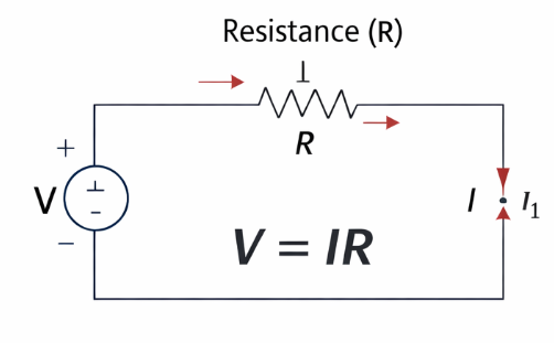
Here, V is the voltage across the resistor, I is the current through it, and R is the resistance. This relationship forms the basis for analyzing almost all electrical circuits.
1.2 Kirchhoff’s Laws
Kirchhoff’s Current Law (KCL)
Kirchhoff’s Current Law states that the algebraic sum of currents at a junction is zero. In simple terms, the total current entering a node must equal the total current leaving that node.
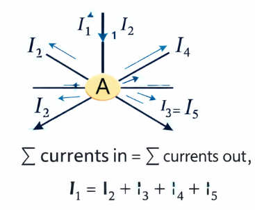
This law is based on the conservation of charge and is widely used in nodal analysis.
Kirchhoff’s Voltage Law (KVL)
Kirchhoff’s Voltage Law states that the algebraic sum of all voltages around any closed loop in a circuit is zero.
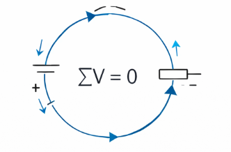
This law follows from the conservation of energy and is essential for loop or mesh analysis.
1.3 Resistors in Series and Parallel
Resistors connected in series share the same current, and their equivalent resistance is the sum of individual resistances:
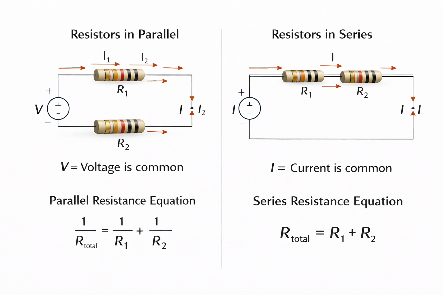
Resistors connected in parallel share the same voltage. The equivalent resistance is given by:
1.4 Voltage Divider Circuit
A voltage divider is a simple yet powerful circuit used to obtain a desired fraction of an input voltage using two resistors in series. The output voltage is given by:
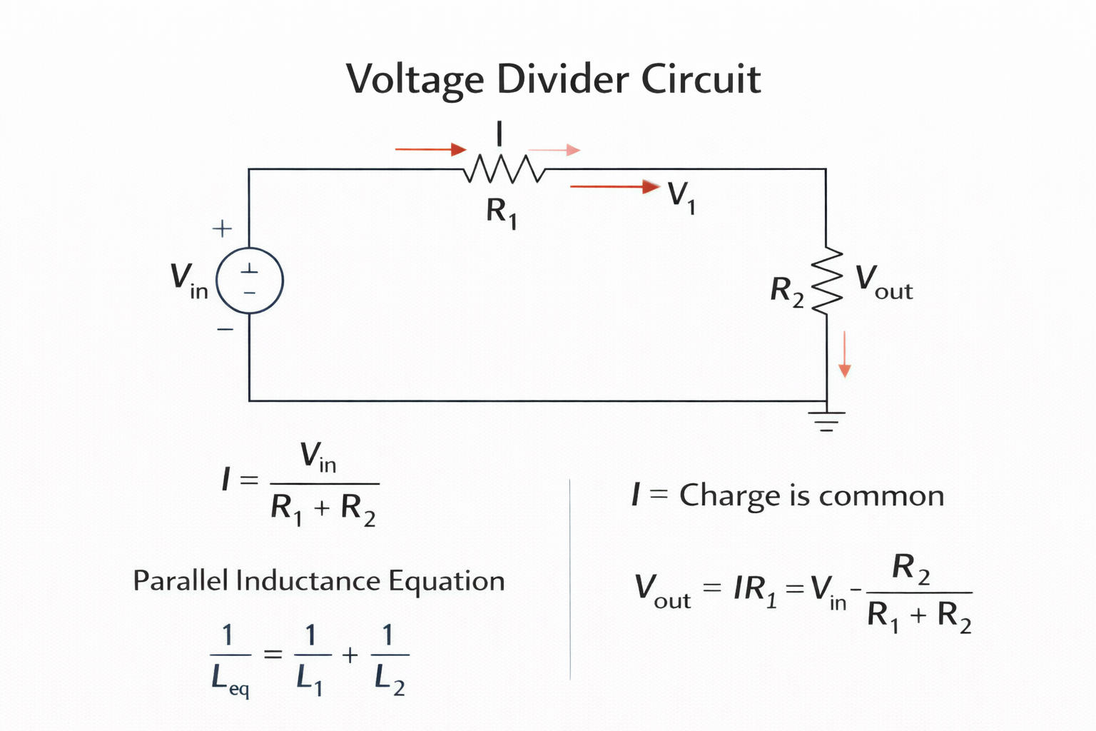
Voltage dividers are widely used in biasing and reference voltage generation.
2. Energy Storage Elements
2.1 Capacitors
A capacitor stores energy in the form of an electric field between two conductive plates separated by a dielectric. The capacitance is given by:
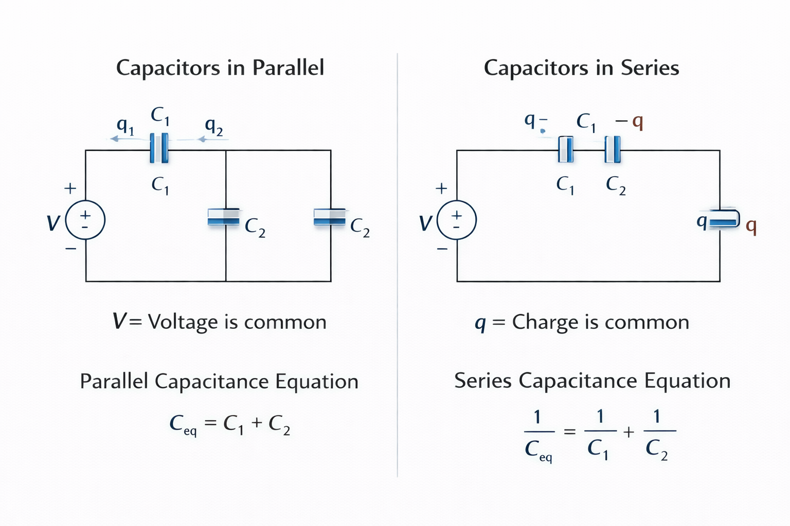
Capacitors oppose sudden changes in voltage and are essential in filtering, timing, and coupling applications. The current-voltage relationship is:
Capacitors can be connected in series or parallel to achieve desired capacitance values.
2.2 Inductors
An inductor stores energy in the form of a magnetic field when current flows through it. Inductors oppose sudden changes in current and are commonly used in filters, transformers, and power electronics.
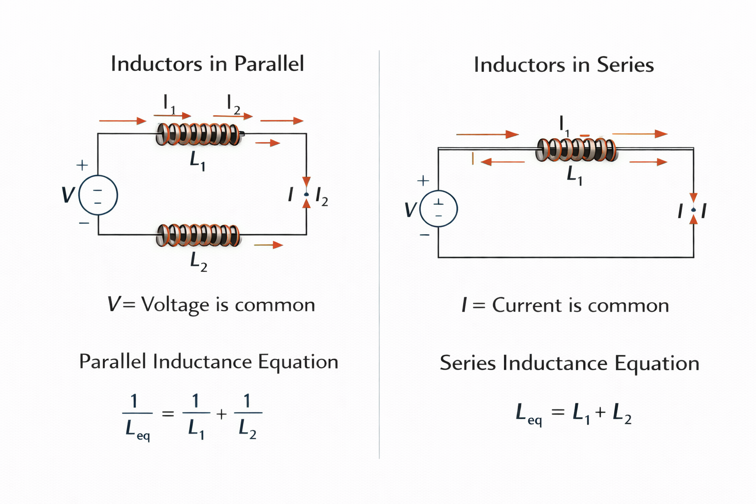
For series-connected inductors:
3. Sources in Circuits
3.1 Voltage Sources
A voltage source maintains a constant voltage independent of the current drawn from it. Ideal voltage sources have zero internal resistance.
3.2 Current Sources
An ideal current source delivers a constant current regardless of the voltage across it. It has infinite output resistance and is mainly used for circuit analysis and biasing concepts.
4. RC Circuits
RC circuits consist of a resistor and capacitor in series. The resistor controls the rate at which the capacitor charges or discharges. The time constant is defined as:
The voltage across the capacitor during charging is:
RC circuits are fundamental in timing, filtering, and signal shaping applications.
Fermi Energy
The value of the Fermi level at absolute zero temperature (–273.15 °C or 0 K) is known as the Fermi Energy. It represents the maximum kinetic energy that an electron can possess at 0 K. For a given solid, the Fermi energy is a fixed value and is a fundamental property of the material.
The highest energy level occupied by electrons at absolute zero temperature is called the Fermi Level. At 0 K, all energy states below the Fermi level are completely filled, and all states above it are completely empty.
In semiconductors and insulators at absolute zero, the Fermi level lies between the valence band and the conduction band. In intrinsic semiconductors, it is approximately at the mid-gap.
The existence of the Fermi level is a direct consequence of Pauli’s Exclusion Principle, which states that no two electrons can occupy the same quantum energy state simultaneously. As a result, electrons fill available energy states starting from the lowest energy upward, leading to a well-defined highest occupied energy level at 0 K.
Fermi Function
The Fermi function f(E) gives the probability of finding an electron in an energy state E at a given temperature. It is derived from Fermi–Dirac statistics and is expressed as:
f(E) = 1 /
where:
E = Energy level
EF = Fermi level
k = Boltzmann constant
T = Absolute temperature (in Kelvin)
At T = 0 K:
- For E < EF, f(E) = 1 (state completely occupied)
- For E > EF, f(E) = 0 (state completely empty)
At temperatures above 0 K, the transition around the Fermi level becomes gradual rather than abrupt, and the probability of occupation follows the Fermi–Dirac distribution curve.
Dependency of Fermi Level on Temperature and Doping Concentration
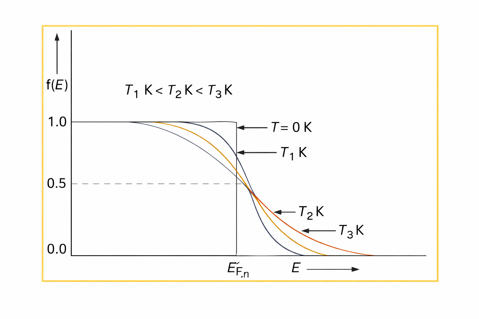
The position of the Fermi level (EF) in a semiconductor depends strongly on both temperature and doping concentration. The behavior can be understood as follows:
- Effect of Temperature on Intrinsic Semiconductor
In an intrinsic semiconductor (pure semiconductor with no intentional doping), the Fermi level lies approximately at the middle of the bandgap at 0 K.
As temperature increases:
- Electron–hole pairs are generated equally.
- Since electron concentration (n) equals hole concentration (p), the Fermi level remains close to the intrinsic Fermi level (Ei).
Hence, for an intrinsic semiconductor, the Fermi level does not significantly shift with temperature; it stays near mid-gap (slight shifts may occur due to effective mass differences, but conceptually it remains centered).
- Doping is Not Applicable for Intrinsic Semiconductor
By definition, an intrinsic semiconductor has no intentional impurities.
Therefore, doping concentration does not apply to intrinsic material. Once doping is introduced, it becomes an extrinsic semiconductor.
- Effect of Pentavalent (Donor) Doping – n-Type Semiconductor
When pentavalent atoms (e.g., P, As) are added:
- Extra electrons are introduced.
- Electron concentration increases significantly.
- The Fermi level shifts upward, toward the conduction band.
As donor concentration increases further:
- EF moves closer to the conduction band edge (EC).
- In heavily doped (degenerate) n-type semiconductors, EF may even enter the conduction band.
- Effect of Trivalent (Acceptor) Doping – p-Type Semiconductor
When trivalent atoms (e.g., B, Al) are added:
- Additional holes (empty states) are created.
- Hole concentration increases.
- The Fermi level shifts downward, toward the valence band.
As acceptor concentration increases:
- EF moves closer to the valence band edge (EV).
- In heavily doped (degenerate) p-type semiconductors, EF may enter the valence band.
- Effect of Increasing Temperature on Extrinsic Semiconductor
In an extrinsic semiconductor at low temperature:
- Carrier concentration is dominated by dopants.
- EF is near EC (n-type) or EV (p-type).
As temperature increases:
- Thermally generated intrinsic carriers increase rapidly.
- Intrinsic carrier concentration (ni) becomes comparable to or greater than doping concentration.
At sufficiently high temperature:
- The semiconductor behaves like an intrinsic semiconductor.
- This is called intrinsic region operation.
- Critical Temperature and Intrinsic Behavior
At a certain high temperature (sometimes referred to as intrinsic transition temperature):
- Intrinsic carrier generation dominates over dopant contribution.
- The extrinsic semiconductor effectively behaves as intrinsic.
- The Fermi level shifts back toward the intrinsic Fermi level (Ei), near the middle of the bandgap.
Thus, temperature tends to push the Fermi level toward mid-gap, while doping pushes it toward conduction band (n-type) or valence band (p-type).
CMOS Expert Insight
From a device physics perspective:
- EF position directly controls carrier concentration through exponential relationships.
- Small shifts in EF can cause large changes in conductivity.
- In advanced CMOS nodes, heavy channel doping, body biasing, and temperature variation significantly impact threshold voltage (Vth), which is strongly related to Fermi level position.
Understanding Fermi level movement is fundamental to analyzing leakage current, threshold voltage variation, and temperature-dependent behavior in modern CMOS technologies.
| Feature | Drift Current | Diffusion Current |
|---|---|---|
| Cause | Applied Electric Field | Concentration Gradient |
| Direction | Same as E-field (holes), Opposite (electrons) | High to Low Concentration |
| Governing Law | Ohm's Law ( | Fick's Law ( |
| Medium | Requires an Electric Field | Occurs even without E-field |
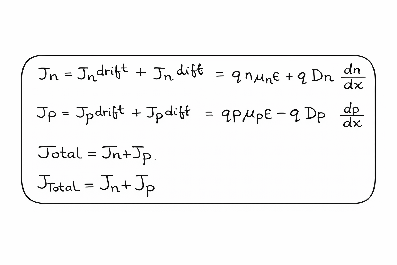
Summary
Diffusion current arises due to the concentration gradient of majority charge carriers in a semiconductor. Whenever there is a difference in carrier concentration between two regions, carriers naturally move from the region of higher concentration to the region of lower concentration. This movement results in diffusion current.
In a P-type semiconductor, diffusion occurs due to the motion of holes. Since holes are the majority carriers, they move from the P-region (high hole concentration) toward the N-region (low hole concentration). Hence, the diffusion current direction is from P to N.
In an N-type semiconductor, diffusion occurs due to the motion of electrons. Electrons move from the N-region (high electron concentration) toward the P-region (low electron concentration). Hence, the diffusion current direction is from N to P.
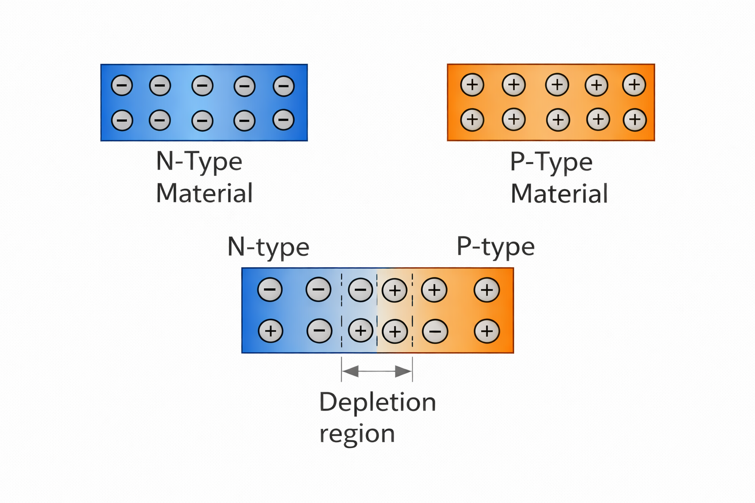
Because of diffusion, charge separation takes place near the junction. This creates an electric field directed from the N-region toward the P-region. This internally generated electric field opposes further diffusion and leads to the formation of the depletion region in a PN junction.
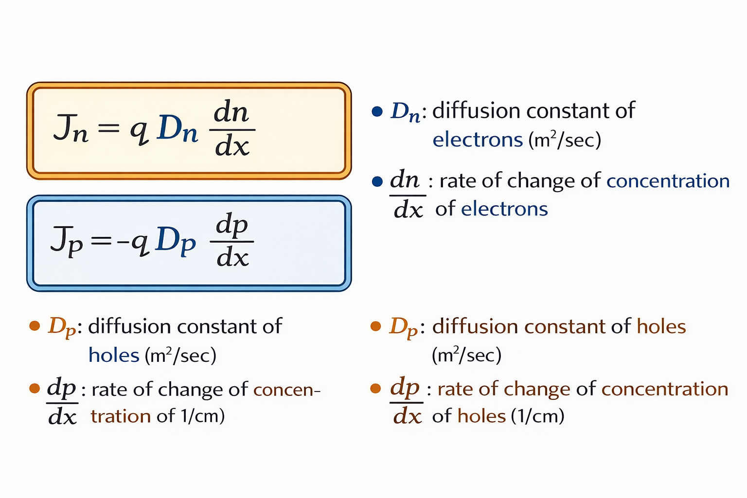
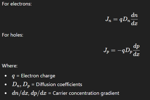
Diffusion current density of electrons is given by Fick’s law as:
Jn(diff) = q Dn (dn/dx)
where:
Jn(diff) = Electron diffusion current density
q = Charge of an electron
Dn = Electron diffusion coefficient
dn/dx = Gradient of electron concentration
Similarly, the hole diffusion current density is:
Jp(diff) = − q Dp (dp/dx)
where Dp is the hole diffusion coefficient and dp/dx is the hole concentration gradient.
Drift Current
Drift current is the current produced due to the motion of charged particles (electrons or holes) under the influence of an externally applied electric field. When an electric field is applied across a semiconductor material, charge carriers experience a force and begin to move with an average velocity known as drift velocity. This movement of carriers results in drift current.
The magnitude of the drift current depends on:
- The strength of the applied electric field
- The number of charge carriers available
- The mobility of carriers
In a PN junction, the applied electric field affects the width of the depletion region. Under reverse bias, the electric field increases and the depletion width widens. Under forward bias, the electric field reduces and the depletion width narrows. Drift current plays a significant role particularly under reverse bias conditions.
Summary
Drift current arises due to the potential gradient (electric field) present in the semiconductor.
In a PN junction under reverse bias, drift current is mainly due to minority charge carriers (electrons in P-region and holes in N-region).
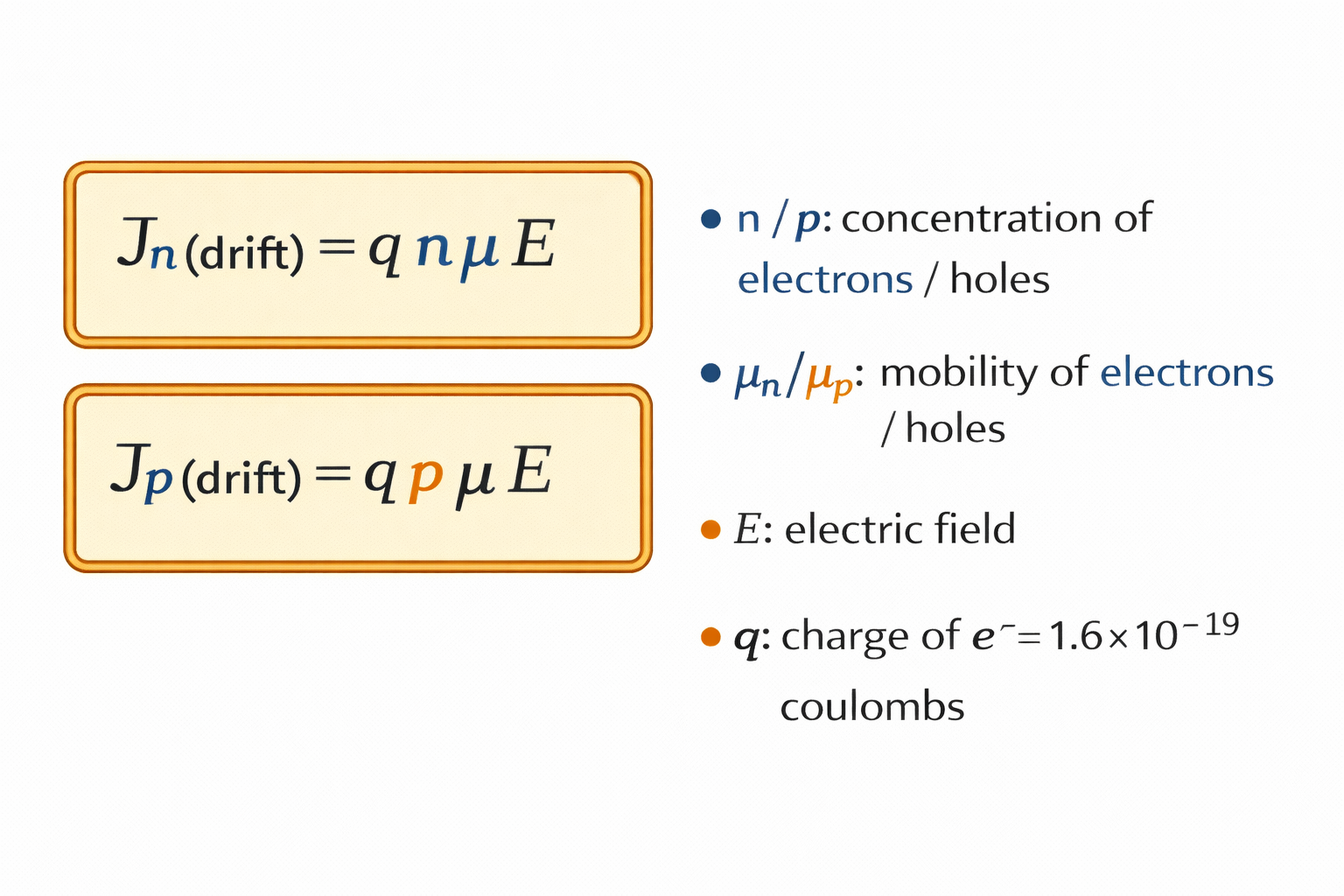
The current density associated with the drift of electrons due to an applied electric field is given by:
Jn(drift) = q n μn E
where:
Jn(drift) = Electron drift current density
q = Electronic charge
n = Electron concentration
μn = Electron mobility
E = Applied electric field
Similarly, for holes:
Jp(drift) = q p μp E
where μp is the hole mobility and p is the hole concentration.
From a device physics standpoint, drift current is directly proportional to the electric field and carrier mobility, and it forms the basis of Ohm’s law in semiconductors.
Why Silicon is Preferred Over Germanium
Silicon (Si) is widely used in semiconductor device fabrication instead of Germanium (Ge) due to the following reasons:
1. Energy Band Gap
- Bandgap of Silicon (Si) ≈ 1.12 eV (at 300K)
- Bandgap of Germanium (Ge) ≈ 0.66 eV (at 300K)
A larger bandgap in silicon results in:
- Lower intrinsic carrier concentration
- Better high-temperature operation
- Reduced leakage current
2. Lower Thermal Carrier Generation
- Due to its larger bandgap, silicon has lower thermal generation of electron-hole pairs
- This improves device stability and reliability
3. Formation of Native Oxide (SiO₂)
- Silicon forms a high-quality native oxide layer (SiO₂)
- SiO₂ is:
- An excellent insulator
- Chemically stable
- Thermally stable
- This property makes MOS technology possible
- One of the biggest reasons CMOS technology is based on silicon
Germanium does not form a stable native oxide suitable for device fabrication.
4. Abundance in Nature
- Silicon is the second most abundant element in Earth’s crust
- Germanium is comparatively rare and expensive
5. Lower Noise
- Silicon devices exhibit lower leakage and lower noise
- More suitable for analog and mixed-signal applications
6. Industrial Ecosystem
Silicon supports fabrication of:
- Resistors
- Capacitors
- Diodes
- Tunnel diodes
- Varactor diodes
- BJTs
- MOSFETs
- CMOS ICs
Hence, Silicon dominates modern semiconductor manufacturing.
Diffusion Current in Semiconductors
Definition
Diffusion current is the current in a semiconductor caused by the movement of charge carriers (electrons and holes) due to concentration gradient, without any external electric field.
It occurs because charge carriers move from:
- High concentration region → Low concentration region
PN Junction Formation and Diffusion
Consider:
N-Type Semiconductor
- Majority carriers: Electrons
- Minority carriers: Holes
P-Type Semiconductor
- Majority carriers: Holes
- Minority carriers: Electrons
When N-type and P-type materials are brought together:
- Electrons diffuse from N → P
- Holes diffuse from P → N
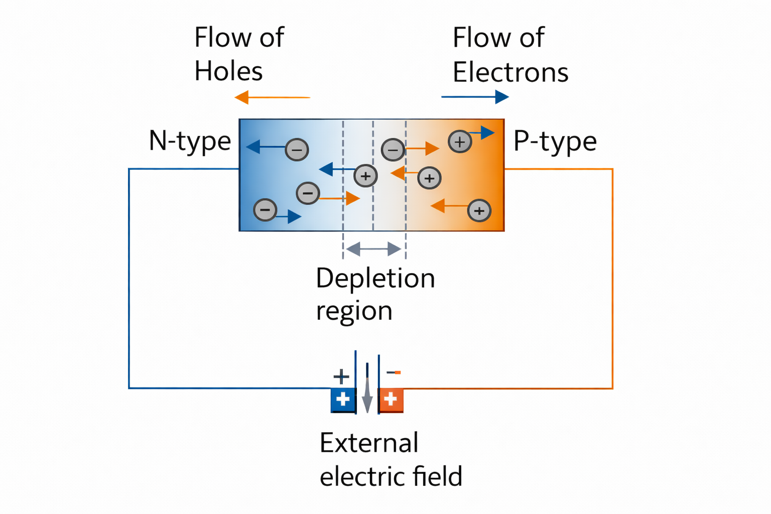
This movement happens due to concentration difference.
Depletion Region
The region near the junction where:
- Mobile charge carriers recombine
- Ions are left behind
- An internal electric field is created
is called the Depletion Region.
Diffusion Current
The current formed due to this carrier movement without external voltage is called:
Diffusion Current
It exists because of non-uniform carrier concentration.
Diffusion Current Density Equations
P-Type Semiconductor – Boron Doping in Germanium
Example: Boron Doping in Germanium
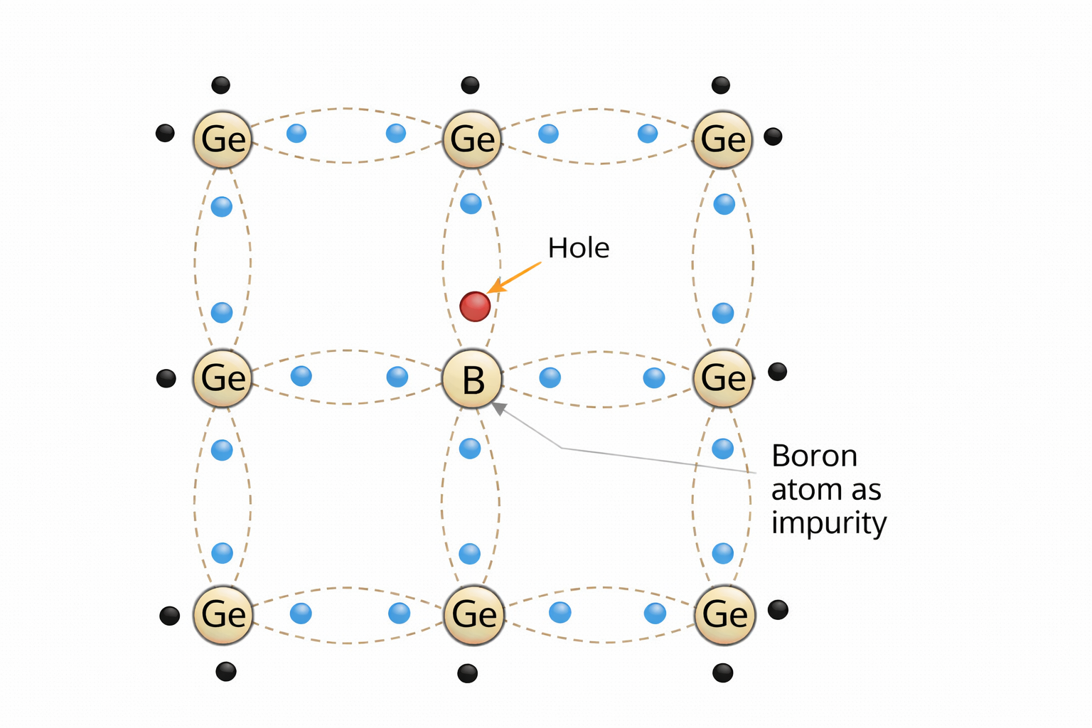
Let us consider that a Boron (B) atom is added to a Germanium (Ge) crystal lattice.
Boron is a trivalent impurity (it has 3 valence electrons). When it replaces a Germanium atom in the lattice:
- Three of the valence electrons of Boron form three covalent bonds with neighboring Germanium atoms.
- However, one bond remains incomplete because Boron has only three valence electrons.
- The missing electron in the fourth bond creates an empty space known as a hole.
This hole behaves as a positive charge carrier.
When Boron impurities are added in small amounts, they generate a large number of holes. These holes contribute to electrical conduction.
All these holes together form what is called the
hole current
.
P-Type Extrinsic Semiconductor
In a P-type semiconductor, conduction occurs primarily through holes.
- Holes are the majority carriers.
- Electrons are the minority carriers.
The trivalent impurity (Boron) creates holes and is therefore called an acceptor impurity, because it accepts electrons from neighboring Germanium atoms.
The number of mobile holes is equal to the number of acceptor atoms added. Hence, the semiconductor remains electrically neutral.
Behavior Under Applied Electric Field
When an external electric field is applied:
- Holes move toward the negative terminal.
- The movement of holes constitutes P-type conductivity.
- Hole movement is slower compared to electron movement.
In reality, conduction happens because valence electrons jump from one covalent bond to another, making it appear as though holes are moving.
This mechanism is different from N-type conduction, where electrons are the majority carriers.
Why Silicon is Preferred Over Germanium?
Among semiconductor materials like Germanium (Ge) and Silicon (Si), Silicon is widely preferred for the manufacture of electronic components for the following reasons:
- Silicon has a larger bandgap (≈ 1.1 eV) compared to Germanium (≈ 0.7 eV).
- Lower leakage current.
- Better thermal stability.
- Easy formation of high-quality SiO₂ layer (important for MOS devices).
- Abundant availability in nature.
- Lower noise in electronic circuits.
Because of these advantages, Silicon is extensively used in the fabrication of:
- Diodes
- Transistors
- BJTs
- MOSFETs
- Integrated Circuits (ICs)
Extrinsic Semiconductors
An impure semiconductor formed by doping a pure (intrinsic) semiconductor with controlled impurities is called an extrinsic semiconductor.
Depending on the type of impurity added, extrinsic semiconductors are classified into:
- N-Type Extrinsic Semiconductor
- P-Type Extrinsic Semiconductor
N-Type Semiconductor
When a small amount of pentavalent impurity is added to a pure semiconductor (such as Silicon or Germanium), it forms an N-type extrinsic semiconductor.
A pentavalent impurity atom has five valence electrons.
Example: Arsenic Doped Germanium
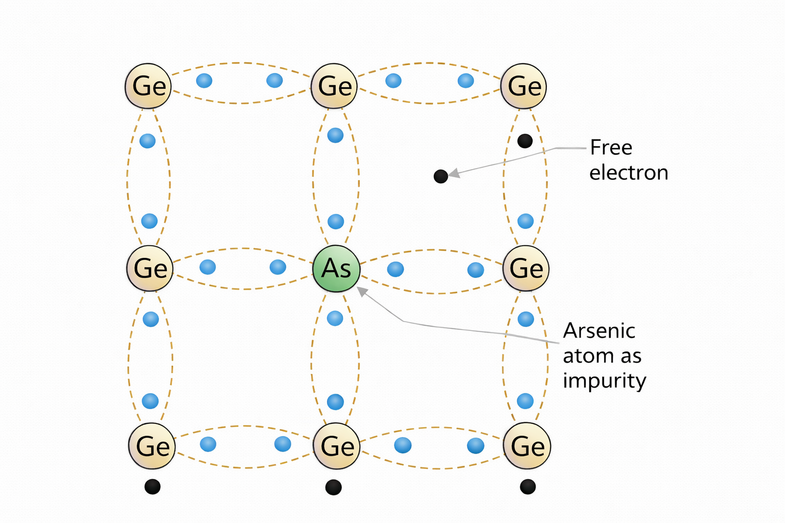
Let us consider that an Arsenic (As) atom is added to a Germanium (Ge) crystal.
- Arsenic has five valence electrons.
- Four of these electrons form covalent bonds with neighboring Germanium atoms.
- One electron remains loosely bound.
- This extra electron becomes a free electron available for conduction.
All such free electrons collectively form the electron current.
Thus, the impurity added provides additional free electrons for conduction.
Characteristics of N-Type Semiconductor
- Conduction takes place mainly through electrons.
- Electrons are the majority carriers.
- Holes are the minority carriers.
- The semiconductor remains electrically neutral because no net positive or negative charge is added.
- When an external electric field is applied:
- Free electrons move toward the positive terminal.
- This conduction mechanism is called N-type conductivity.
Donor Impurity
Pentavalent atoms are called donor atoms because they donate one extra electron to the conduction band of the semiconductor.
Common pentavalent impurities include:
- Arsenic (As)
- Phosphorus (P)
- Antimony (Sb)
P-Type Semiconductor
When a small amount of trivalent impurity is added to a pure semiconductor, it forms a P-type extrinsic semiconductor.
A trivalent impurity atom has three valence electrons.
Trivalent Impurities
Trivalent impurities have three valence electrons in their outermost shell.
Examples:
- Boron (B)
- Gallium (Ga)
- Indium (In)
- Aluminum (Al)
Acceptor Impurity
Trivalent atoms are called acceptor atoms because:
- They accept one electron from the semiconductor atom.
- This creates a hole in the valence band.
- The hole acts as a positive charge carrier.
In a P-type semiconductor:
- Holes are the majority carriers.
- Electrons are the minority carriers.
- Conduction occurs mainly through hole movement.
Intrinsic Semiconductors
An intrinsic semiconductor is the pure form of a semiconductor material without any intentional doping. In this type of material, the electrical properties are solely determined by the semiconductor itself, such as Silicon (Si) or Germanium (Ge).
Key Properties of Intrinsic Semiconductors
- Electron–Hole Pair (EHP) Generation
Charge carriers (electrons and holes) are generated due to thermal excitation. When thermal energy is supplied, some valence electrons gain enough energy to move to the conduction band, leaving behind holes in the valence band. - Equal Number of Electrons and Holes
In an intrinsic semiconductor:
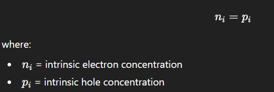
Since no impurity atoms are added, the number of free electrons is equal to the number of holes.
- Low Conductivity at Room Temperature
The conduction in intrinsic semiconductors is relatively small at room temperature because the number of thermally generated carriers is limited. - Insulating Behavior at 0°C (Approximately Absolute Zero)
At very low temperatures, particularly near absolute zero, there is no thermal energy available to excite electrons. Hence, no free charge carriers are present, and the material behaves like an insulator. - Continuous Generation and Recombination
Electron–hole pair generation and recombination is a continuous process due to thermal agitation.
- Generation: Thermal energy creates electron–hole pairs.
- Recombination: Free electrons recombine with holes, releasing energy.
Important Definitions
- Intrinsic Carrier Concentration (nin_ini)
The intrinsic carrier concentration refers to the concentration of charge carriers (electrons or holes) in a pure semiconductor material.
Since:
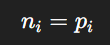
The intrinsic carrier concentration represents both intrinsic electron and intrinsic hole concentrations.
In summary, intrinsic semiconductors are electrically neutral materials in which conduction occurs purely due to thermally generated electron–hole pairs, without the influence of impurity atoms.